Tunneling enhancement type HEMT device
An enhanced, tunneling technology, used in semiconductor devices, electrical components, circuits, etc., can solve problems such as damage to the material of the barrier layer, reduction of forward current capability, and impact on the reliability of carrier mobility devices. The effect of reducing the effective area
- Summary
- Abstract
- Description
- Claims
- Application Information
AI Technical Summary
Problems solved by technology
Method used
Image

Examples
Embodiment 1
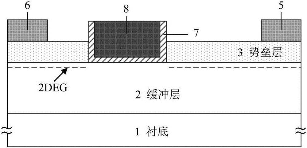
[0035] Such as Figure 5 As shown, this example includes a substrate 1, a buffer layer 2 located on the upper layer of the substrate 1, and a barrier layer 3 located on the upper layer of the buffer layer 2. The contact surface between the buffer layer 2 and the barrier layer 3 forms a two-dimensional electron gas (2DEG) the first heterojunction of the channel; one end of the upper surface of the barrier layer 3 has a drain electrode 5 in ohmic contact; the other end of the upper surface of the barrier layer 3 has a source electrode of Schottky contact 6. The upper surface of the barrier layer 3 has a reverse polarized semiconductor layer 4, and the contact surface between the reverse polarized semiconductor layer 4 and the barrier layer 3 forms a second heterojunction with two-dimensional hole gas (2DHG) The source electrode 6 is connected to the reverse polarized semiconductor layer 4 and extends toward the direction close to the drain electrode 5 along the upper surface of ...
Embodiment 2
[0038] This example is a polarized superjunction tunneling enhanced HEMT device with step doping. Compared with Example 1, this example adopts different types or concentrations of doping in different regions in the anti-polarization semiconductor layer 4, and other structures are the same as Embodiment 1 is the same, as Image 6 shown. On the one hand, the concentration of 2DHG can be changed by doping, so that the depletion part of the drift region can be further expanded; on the other hand, when step doping is used in the anti-polarization semiconductor layer 4, a new electric field can be introduced at the interface of different doped regions The peak, further optimizes the lateral electric field distribution in the device drift region, and improves the device withstand voltage in the blocking state.
Embodiment 3
[0040] This example is a polarized superjunction tunneling enhanced HEMT device that uses ion implantation to block holes. Compared with Example 1, this example uses a high concentration of N between the reverse polarized semiconductor layer 4 and the drain electrode 5. Type ion implantation realizes the hole blocking region 9, avoiding the formation of hole conduction channels between the source and the drain; at the same time, P-type doping is used in the semiconductor layer near the source, and the P-type doping prevents electrons from flowing from the source To the conduction path of the drain, other structures are the same as in Embodiment 1, such as Figure 7 shown. The NP junction formed between the drain electrode and the source electrode also plays the role of withstand voltage when the device is in the blocking state. The isolation methods in conventional HEMT devices mainly include trench isolation and ion implantation isolation. Compared with trench isolation, ion...
PUM
 Abstract
Description
Claims
Application Information