Enhancement mode HEMT (high electron mobility transistor) device

An enhanced and device technology, applied in semiconductor devices, electrical components, circuits, etc., can solve problems such as gate leakage, barrier layer material damage, and difficulty in controlling the distribution of fluorine ions, and achieve the effect of facilitating control and reducing the effective area

Active Publication Date: 2015-12-09
UNIV OF ELECTRONICS SCI & TECH OF CHINA
View PDF3 Cites 20 Cited by
  • Summary
  • Abstract
  • Description
  • Claims
  • Application Information

AI Technical Summary

Problems solved by technology

However, implanting fluorine ions in the barrier layer will cause damage to the material of the barrier layer on the one hand; on the other hand, the thinner barrier layer makes the distribution of fluorine ions difficult to control, and the fluorine ions located in the barrier layer are far away from the 2DEG trench. If the channel is very close, the concentration and mobility of electrons in the channel will be reduced, which will eventually greatly affect the current capability of the device and cause a decrease in reliability.
The literature (AkiraNakajima, et.al. "GaN-BasedSuperHeterojunctionFieldEffectTransistorsUsingthePolarizationJunctionConcept" IEEE ElectronDeviceLetters, vol.32, no.4, pp.542-544, 2011) adopts the idea of ​​a polarized superjunction, growing above the AlGaN barrier layer in the drift region A top layer of GaN, and two-dimensional hole gas (2DHG) is formed at its interface. The 2DHG and the 2DEG below form a natural "superjunction". So as to achieve the purpose of improving the withstand voltage, such as Figure 4 As shown, but the top layer of GaN and the gate electrode form an ohmic contact of holes, and when the forward conduction is conducted, the gate leakage current will be generated when the gate voltage is large, which limits the gate voltage swing.

Method used


Image

  • Enhancement mode HEMT (high electron mobility transistor) device
  • Enhancement mode HEMT (high electron mobility transistor) device
  • Enhancement mode HEMT (high electron mobility transistor) device

Examples


Embodiment 1

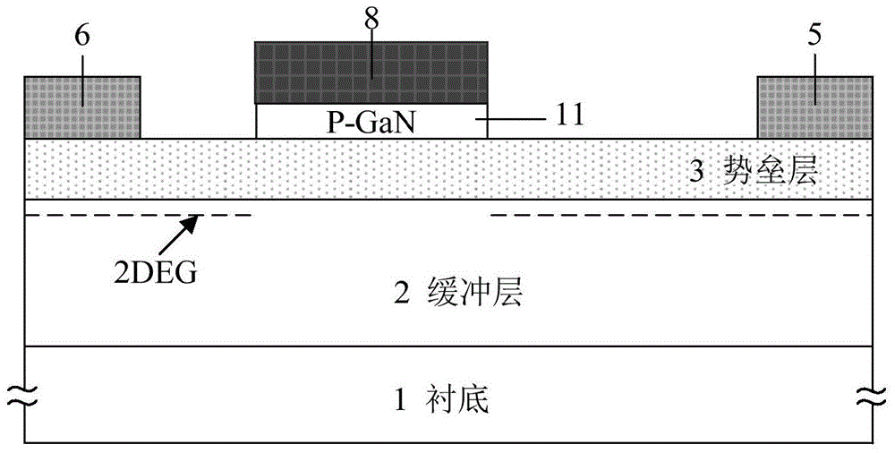
[0037] like Figure 5 As shown, it includes a substrate 1, a buffer layer 2 located on the upper layer of the substrate 1 and a barrier layer 3 located on the upper layer of the buffer layer 2, and the contact surface between the buffer layer 2 and the barrier layer 3 is formed with a two-dimensional electron gas (2DEG ) the first heterojunction of the channel; one end of the upper surface of the barrier layer 3 has a drain electrode 5 that forms ohmic contact with the barrier layer 3; it is characterized in that the upper surface of the barrier layer 3 has a A reversely polarized reverse polarization semiconductor layer 4, the contact surface of the reverse polarization semiconductor layer 4 and the barrier layer 3 forms a second heterojunction with two-dimensional hole gas (2DHG); the reverse polarization One end of the upper surface of the semiconductor layer 4 away from the leakage current 5 has a source electrode 6, and the connection interface between the source electrod...

Embodiment 2

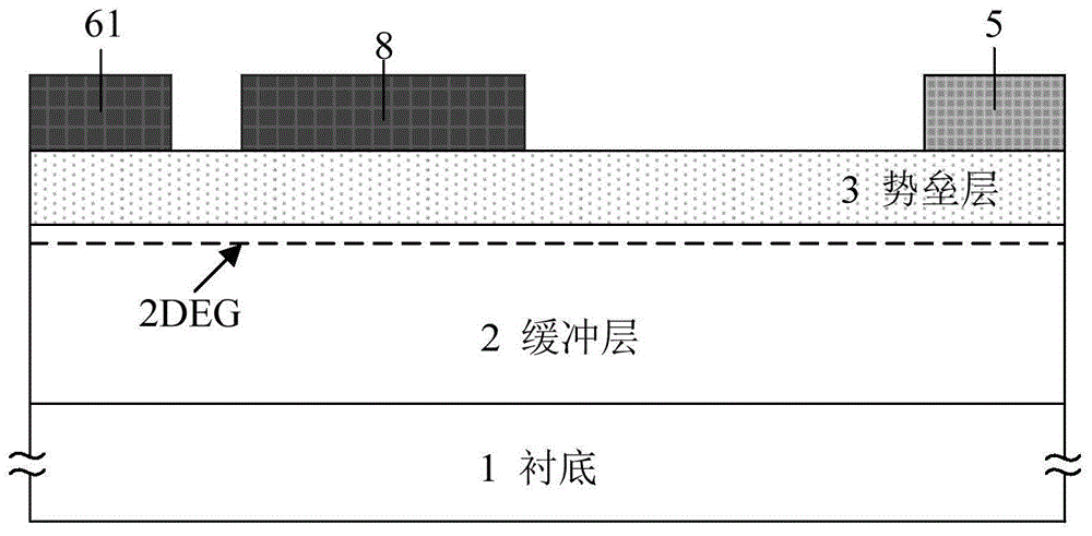
[0040] This example is a polarized superjunction tunneling enhanced HEMT device that uses ion injection to block holes. Compared with Example 1, the device of this example uses a high concentration of N between the reverse polarization layer 4 and the drain electrode 5. The hole blocking region 9 is realized by ion implantation, avoiding the formation of a hole conduction channel between the source and the drain; at the same time, a P-type doped region is formed in a part of the reverse polarized layer between the source and the drain to prevent electrons from Leakage path from source to drain, other structures are the same as in Example 1, such as Image 6 shown. The NP junction formed between the drain electrode and the source electrode also plays the role of withstand voltage when the device is in the blocking state. The isolation methods in conventional HEMT devices mainly include trench isolation and ion implantation isolation. Compared with trench isolation, ion implant...

Embodiment 3

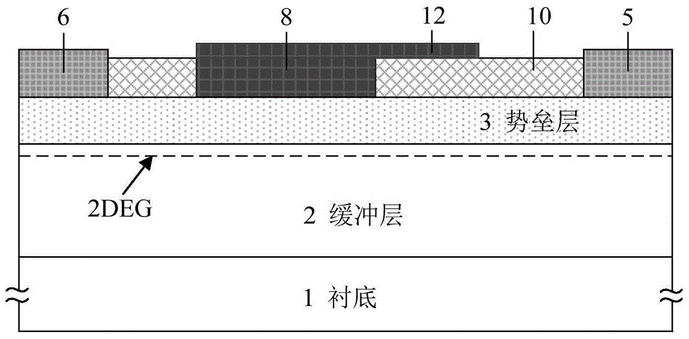
[0042] This example is an enhancement mode HEMT device in which the part of the reverse polarized layer located under the source electrode adopts N-type doping. type doping, other structures are the same as in Example 1, such as Figure 7 shown. On the one hand, the N-type doping part under the source electrode can better form ohmic contact between the source metal and the reverse polarized layer; on the other hand, the N-type doping modulates the 2DHG concentration, thereby regulating the threshold voltage; Step doping or linear doping can be performed on other parts of the polarization layer to further optimize the lateral electric field distribution in the drift region of the device and improve the withstand voltage.


PUM


Abstract

The invention belongs to the technical fields of semiconductors, and particularly relates to an enhancement mode HEMT (high electron mobility transistor) device. According to the enhancement mode HEMT device, a reverse polarization layer is grown on the upper surface of a barrier layer between a grid electrode and a drain electrode; the reverse polarization layer and the barrier layer produce reverse polarization to form two-dimensional hole gas (2DHG) in heterojunction interface; the reverse polarization layer, barrier layer, buffering layer form polarization super junctions; meanwhile, a metal grid electrode is not positioned between a source electrode and the drain electrode any more, instead, an insulation gate electrode is formed by etching a groove in the edge of the source edge far from the drain electrode; on one hand, longitudinal conductive channels between the source electrode and two-dimensional electron gas (2DEG) are cut by the 2DHG; the magnetic field control on the conductive channels is realized by applying voltage on the groove gate electrode so as to realize the enhancement mode; and the regulation and control on the threshold value voltage can be realized by doping parts of the conductive channels; and on the other hand, the polarization super junctions between the gate electrode and the drain electrode assist to use up a drifting region in a blocked state so as to optimize the transverse electric field distribution of the device and improve the voltage resistance of the device.

Description

technical field [0001] The invention belongs to the technical field of semiconductors, and in particular relates to an enhanced HEMT (High Electron Mobility Transistor, high electron mobility transistor) device. Background technique [0002] The wide-bandgap semiconductor gallium nitride (GaN) has the characteristics of high critical breakdown electric field (~3.3×10⁶V / cm), high electron mobility (~2000cm2 / V s), and the heterojunction based on GaN material has high electron The mobility transistor (HEMT) also has a high concentration (~1013cm-2) of two-dimensional electron gas (2DEG), which makes the GaN HEMT device have the characteristics of high reverse blocking voltage, low forward conduction resistance, and high operating frequency. , Low power consumption, high voltage switching device application field has huge application prospects. [0003] For AlGaN / GaN HEMT devices, enhancement-mode (normally-off) HEMT devices have more advantages than depletion-mode (normally-on...

Claims


Application Information

Patent Timeline
Patent Type & Authority Applications(China)
IPC IPC(8): H01L29/10H01L29/778
CPCH01L29/1025H01L29/778H01L29/41775H01L29/4236H01L29/7786H01L29/0646H01L29/0653H01L29/0847H01L29/2003H01L29/205
Inventor 罗小蓉熊佳云杨超魏杰吴俊峰彭富张波
Owner UNIV OF ELECTRONICS SCI & TECH OF CHINA
Why Eureka
Try Eureka