MEMS sensor packaging structure and method

A packaging method and packaging structure technology, which are applied in microstructure devices, processing microstructure devices, microstructure technology, etc., can solve problems such as large differences in thermal expansion coefficients, deformation of MEMS sensor chips, and effects on the performance of MEMS sensor chips. , to reduce the impact and improve the overall performance

Inactive Publication Date: 2015-12-09
INST OF GEOLOGY & GEOPHYSICS CHINESE ACAD OF SCI
View PDF12 Cites 20 Cited by
  • Summary
  • Abstract
  • Description
  • Claims
  • Application Information

AI Technical Summary

Problems solved by technology

Most of the current mainstream MEMS sensor chips are made of silicon materials, while the ceramics used in traditional ceramic packaging methods are mostly alumina and aluminum nitride. The thermal expansion coefficient of this material and the material (silicon) of MEMS sensor chips is quite different. , when the temperature of the packaged or packaged device changes, different materials shrink or expand in different degrees, and the resulting stress mismatch will cause deformation of the package shell of the MEMS sensor chip and the MEMS chip itself, thereby affecting the MEMS sensor chip. The performance of the sensor chip device, or even directly lead to the failure of the MEMS sensor chip device

Method used


Image

  • MEMS sensor packaging structure and method
  • MEMS sensor packaging structure and method
  • MEMS sensor packaging structure and method

Examples


Embodiment Construction

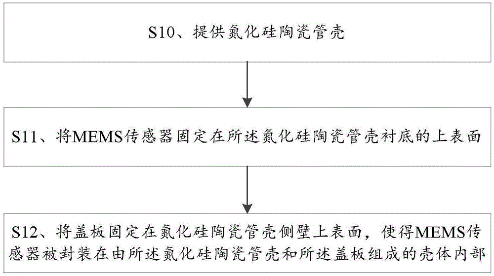
[0036] The technical solution of the present application will be further described in detail below in conjunction with the accompanying drawings.

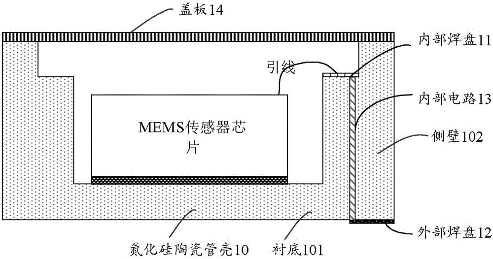
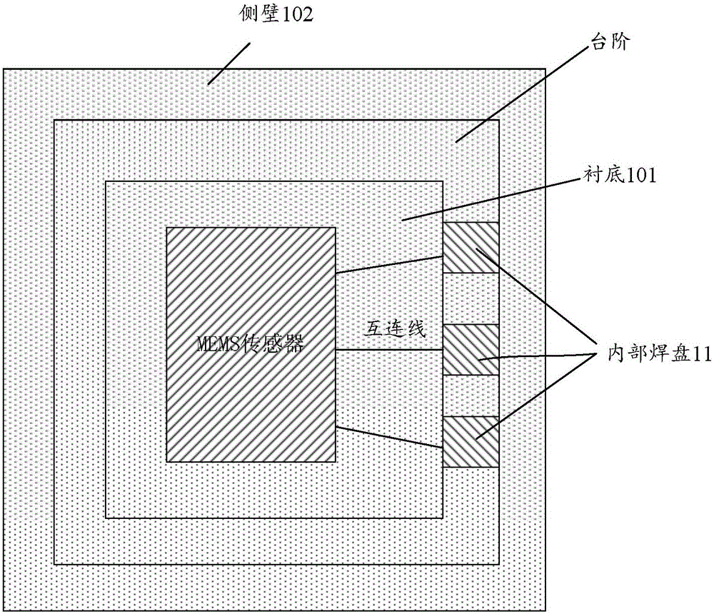
[0037] figure 1 Is a cross-sectional view of a MEMS sensor packaging structure according to an embodiment of the present application, figure 2 It is a schematic top view of the MEMS sensor package structure according to an embodiment of the present application with the cover plate removed. The packaging structure of the MEMS sensor is used to package a MEMS sensor chip made of silicon material, such as an inertial sensor made of silicon material, including a gyroscope or an accelerometer. The packaging structure includes: a silicon nitride ceramic package 10, an internal pad 11, an external pad 12, an internal circuit 13, and a cover plate 14.

[0038] Wherein, the silicon nitride ceramic package 10 includes a substrate 101 and sidewalls 102, and the substrate 101 is used to fix a MEMS sensor chip. The side wall 102 located inside the...


PUM


Abstract

The invention provides an MEMS sensor chip packaging structure and method. The packaging structure comprises a silicon nitride ceramic tube shell, an internal bonding pad, an external bonding pad, an internal circuit and a cover plate, wherein the silicon nitride ceramic tube shell comprises a substrate and sidewalls; the substrate is used for fixing an MEMS sensor chip and the sidewall located on the inner side of the silicon nitride ceramic tube shell is provided with a step; the internal bonding pad is located on the upper surface of the step and connected with the signal output end of the MEMS sensor chip; the external welding pad is located on the outer surface of the silicon nitride ceramic tube shell; the internal circuit is used for connecting the internal welding pad and the external welding pad; the cover plate is partially or completely located within the substrate and the sidewalls and used for sealing the silicon nitride ceramic tube shell. According to the MEMS sensor packaging structure, the influence of packaging thermal stress on the performance of the MEMS sensor chip device is effectively reduced, and therefore, the overall performance of the sensor is improved.

Description

Technical field [0001] This application relates to the technical field of component packaging, and in particular to a packaging structure and packaging method for a MEMS (Micro-Electro-Mechanical System) sensor. Background technique [0002] MEMS (Micro Mechanical System) is an emerging technology developed from traditional integrated circuit technology, which realizes sensing or execution functions by making micron and nano-scale mechanical structures. Because its size is very different from the conventional millimeter or centimeter functional modules, it is necessary to realize the mutual transmission of electrical signals between modules of different scales through packaging. In the process of realizing signal transmission, the packaging itself must It is possible to reduce the impact on the MEMS chip, while also protecting the MEMS chip from external environmental interference factors. [0003] Traditional MEMS sensor chip packaging mainly includes three methods: metal materia...

Claims


Application Information

Patent Timeline
Patent Type & Authority Applications(China)
IPC IPC(8): B81B7/00B81B7/02B81C3/00
Inventor 俞度立
Owner INST OF GEOLOGY & GEOPHYSICS CHINESE ACAD OF SCI
Why Eureka
Try Eureka