Chip-level diamond NV-color center magnetic imaging device and method

A diamond and chip-level technology, which is applied in measurement devices, measurement of magnetic variables, medical science, etc., can solve the problem of ultra-high spatial resolution detection without a good collection and measurement method, and the real-time contradiction between spatial resolution and measurement, which has not been realized. Miniaturized applications and other issues, to achieve the effect of good real-time performance, small size and fast response speed

Active Publication Date: 2015-12-09
BEIHANG UNIV +1
View PDF5 Cites 24 Cited by
  • Summary
  • Abstract
  • Description
  • Claims
  • Application Information

AI Technical Summary

Problems solved by technology

In this context, due to the extremely high spatial resolution achieved by the diamond color center for magnetic field measurement, there is currently no better way to collect and measure it for ultra-high spatial resolution detection
At the same time, it is difficult to achieve miniaturization because it requires laser polarization, temperature and magnetic field environment control
[0003] Based on diamond NV - The magnetic field measurement of the color center has been recognized by the field of magnetic field measurement, and has achieved initial success. Currently, a single NV is mainly used - The color center is used as a magnetic field probe for magnetic field scanning imagi

Method used


Image

  • Chip-level diamond NV-color center magnetic imaging device and method
  • Chip-level diamond NV-color center magnetic imaging device and method
  • Chip-level diamond NV-color center magnetic imaging device and method

Examples


Embodiment Construction

[0022] The present invention will be further described below by means of the accompanying drawings and specific embodiments.

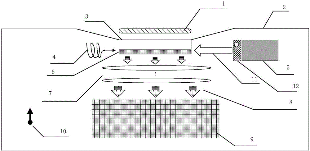
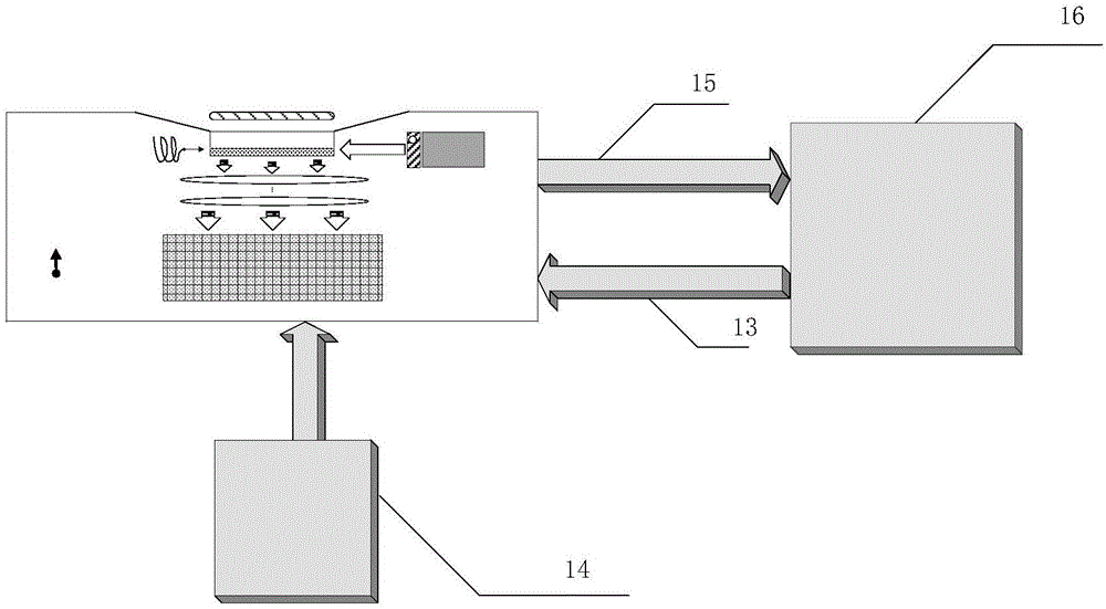
[0023] like figure 1 As shown, a chip-level diamond NV of the present invention - The color center magnetic imaging device includes an external packaging environment 2, containing NV - Color center diamond 3, microwave 4, 532nm laser 5 and laser pulse switch 12, dichroic filter film 6 nano-convex lens 7 groups, distributed optical imaging unit 9, bias magnetic field 10 and polarized laser 11; one layer The dichroic filter film 6 is fabricated on a - The lower surface of the diamond 3 at the color center, the dichroic filter film 6 can block the 532nm polarized laser light 11, and allow the 637nm fluorescent light 8 to pass through; NV - The upper surface of the diamond 3 of the color center is in contact with the sample 1 to be tested, and the bias magnetic field 10 provides an external magnetic ring mirror; the 532nm laser 5 and the laser pulse swi...


PUM


Abstract

The invention discloses a chip-level diamond NV-color center magnetic imaging device and method, and the method achieves the hyperfine magnetic field imaging of the two-dimensional surface of an object, such as a magnetic image of a biological cell. The method comprises the steps: carrying out the polarization of a laser pulse and a microwave pulse; generating fluorescent light generated at the NV-color center of a diamond in an external magnetic field; employing the laser pulse to generate fluorescent light again, wherein the difference result of fluorescent light of two times can reflect the magnetic field intensity of the NV-color center, thereby achieving the conversion of magnetic field information to optical information; and employing a nano-level convex lens group and a distributed optical imaging unit to convert an optical signal into an electric signal. The invention also relates to a packaging method for enabling a whole system to be packaged in a manner of chip level, and the method comprises temperature control and electromagnetic shielding. The method is great in value in the fields of biomedical research and medical diagnosis.

Description

technical field [0001] The present invention designs a chip-level diamond NV - The color center magnetic imaging device and method realize ultra-smart magnetic field imaging of two-dimensional surfaces, which can serve the magnetic image research of biological cells and medical image detection and other related fields. Background technique [0002] In the application process of existing bioimaging technology, due to insufficient detection resolution or detection sensitivity, it is not only difficult to meet the needs of research fields such as living tissue observation and cytopathological analysis, but even delays the early detection of various diseases including cancer. Discovery and treatment. In the existing field of micro-scale imaging, the imaging technologies that can be used for biological imaging can be divided into three types: optical imaging, photoelectric imaging and magnetic field measurement imaging. Among them, optical imaging has the disadvantages of requi...

Claims


Application Information

Patent Timeline
IPC IPC(8): G01R33/10A61B5/05
Inventor 袁珩张冀星张刚源曹传桂肖兴
Owner BEIHANG UNIV
Why Eureka
Try Eureka