A method of manufacturing a semiconductor device with cross-line field plates

A manufacturing method and semiconductor technology, applied in semiconductor/solid-state device manufacturing, semiconductor devices, electrical components, etc., can solve problems such as complex field plate manufacturing methods, and achieve the effects of simple manufacturing methods, balanced electric field distribution, and high processing efficiency

Active Publication Date: 2017-11-10
CHENGDU HIWAFER SEMICON CO LTD
View PDF4 Cites 0 Cited by
  • Summary
  • Abstract
  • Description
  • Claims
  • Application Information

AI Technical Summary

Problems solved by technology

[0003] The object of the present invention is to address the deficiencies in the prior art, to provide a method for manufacturing a semiconductor device with a cross-line field plate, which can well solve the problem of existing semiconductor device field plates. The problem of complex manufacturing methods

Method used


Image

  • A method of manufacturing a semiconductor device with cross-line field plates
  • A method of manufacturing a semiconductor device with cross-line field plates
  • A method of manufacturing a semiconductor device with cross-line field plates

Examples


Embodiment Construction

[0024] In order to make the purpose, technical solution and advantages of the present application clearer, the present application will be further described in detail below in conjunction with the accompanying drawings and specific embodiments. For simplicity, some technical features known to those skilled in the art are omitted from the following description.

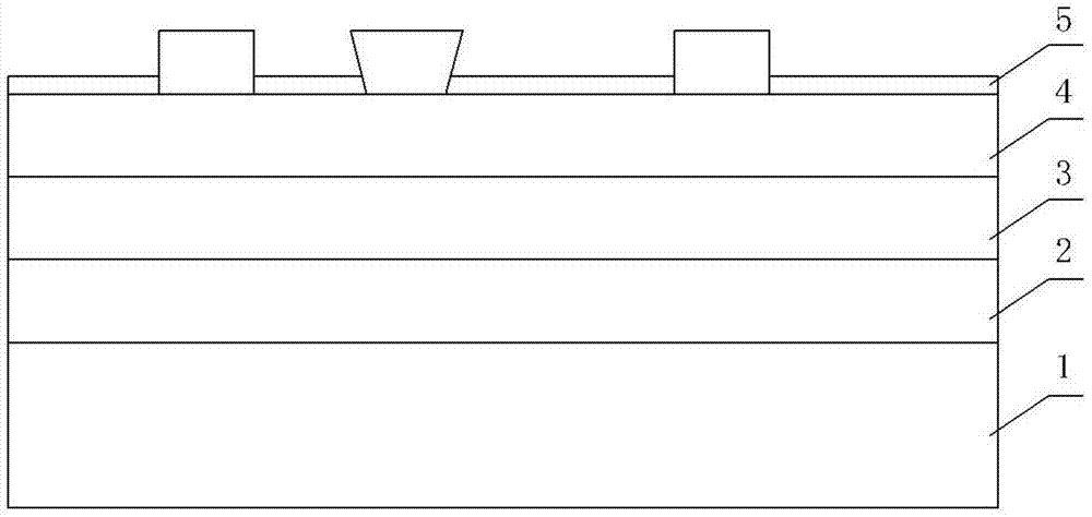
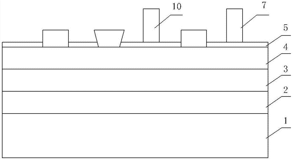
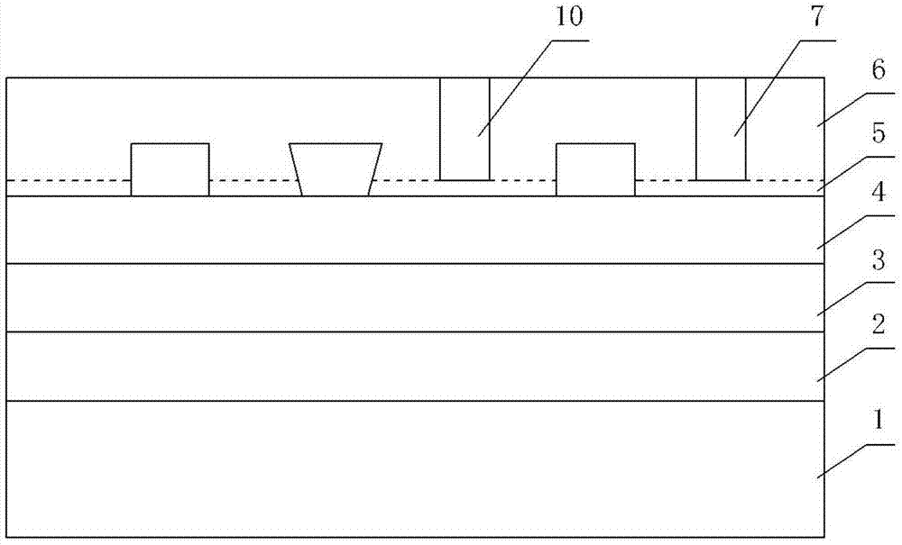
[0025] According to one embodiment of the present invention, a method for manufacturing a semiconductor device with cross-line field plates is provided, a substrate 1 is provided, and a nucleation layer 2, a buffer layer 3, and a barrier layer 4 are sequentially formed on the substrate 1, and the Forming the gate 11, the source 12 and the drain 8 on the barrier layer 4 also includes the following steps:

[0026] S1, such as figure 1 As shown, the first layer of dielectric layer 5 is deposited on the barrier layer 4, and the dielectric layer can be made of SiO2 or SiNX material to allow the subsequent processing of the...


PUM


Abstract

The invention provides a manufacturing method of a semiconductor device with an overline field plate. The method comprises providing a substrate, successively forming a nuclear layer, a buffer layer and a barrier layer on the substrate and forming a grid electrode, a source electrode and a drain electrode on the barrier layer, and further comprises the following steps: S1, depositing a first dielectric layer on the barrier layer; S2, depositing a first vertical field plate of the overline field plate on the first dielectric layer between the grid electrode and the drain electrode, and depositing a second vertical field plate of the overline field plate at one side, which is away from the grid electrode, of the drain electrode or one side, which is away from the grid electrode, of the source electrode; S3, depositing a second dielectric layer on the first dielectric layer, wherein the deposition thickness is the same as the height of the first vertical field plate and the height of the second vertical field plate; and S4, depositing a horizontal field plate of the overline field plate on the second dielectric layer, wherein the horizontal field plate is connected with the first vertical field plate and the second vertical field plate. According to the invention, the manufacturing method is simple, the processing efficiency is high, the processed overline field plate can effectively balance electric field distribution of the root portion of the grid electrode, and the voltage withstanding value of the semiconductor device is improved.

Description

technical field [0001] The invention belongs to the technical field of semiconductor devices, and in particular relates to a method for manufacturing a semiconductor device with cross-line field plates. Background technique [0002] Power semiconductor devices have broad application prospects in the field of power electronics, which can improve equipment efficiency, save energy, increase integration, and reduce equipment volume. Commonly used power semiconductor devices such as GaAs, GaN, SiC and other materials have different withstand voltages. Through the analysis of the working principle of power semiconductor devices, the voltage difference between the gate and the drain is relatively large, and the breakdown position of the device under high voltage is usually at the root of the gate, near the drain. The breakdown of the semiconductor layer, usually the breakdown voltage Below 100V. For the material of the semiconductor layer, taking GaN as an example, the theoretica...

Claims


Application Information

Patent Timeline
Patent Type & Authority Patents(China)
IPC IPC(8): H01L29/78H01L29/40H01L21/336
CPCH01L29/404H01L29/66477H01L29/78
Inventor 李春江
Owner CHENGDU HIWAFER SEMICON CO LTD
Why Eureka
Try Eureka