LED lamp filament illuminating strip and preparation method therefor

A technology of LED filaments and light strips, which is applied in the direction of electrical components, electric solid devices, circuits, etc., can solve the problems of affecting light transmission, uneven light mixing, and hindering heat dissipation, so as to improve the uniformity of light output and reduce Package cost, effect of improving yield rate

Active Publication Date: 2015-12-16
SHANDONG INSPUR HUAGUANG OPTOELECTRONICS
View PDF6 Cites 81 Cited by
  • Summary
  • Abstract
  • Description
  • Claims
  • Application Information

AI Technical Summary

Problems solved by technology

Although the filament achieves 360-degree light emission, the substrate formed of silicone resin containing phosphor and the light-emitting orientation of the chip must meet specific requirements, otherwise uneven light mixing may eventually occur
[0007] Compared with the existing LED filament chip attached to the substrate, the unidirectional continuous distribution on both sides of the substrate, the substrate not only affects the transmission of light, increases the cost, but also hinders the dissipation of heat, and the distribution of the chip affects the uniformity of light. The wire bonding connection of the chip reduces the reliability of the packaging yield

Method used


Image

  • LED lamp filament illuminating strip and preparation method therefor
  • LED lamp filament illuminating strip and preparation method therefor
  • LED lamp filament illuminating strip and preparation method therefor

Examples


Embodiment Construction

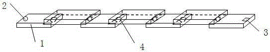
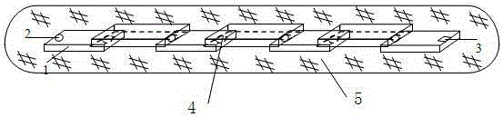
[0027] The LED filament light emitting strip of the present invention is such as image 3 As shown, two rows of LED chips are included, and the lower row of LED chips is arranged on the upper row of LED chips. The LED chips 1 in the lower row are arranged at intervals, and the LED chips in the upper row are respectively overlapped between two adjacent LED chips 1 in the lower row. The LED chips in the lower row are opposite to the light emitting surface of the LED chips in the upper row. The positive electrode and the negative electrode of the LED chip in the upper row are respectively welded to the negative electrode and the positive electrode of the two adjacent LED chips 1 in the lower row to form a chip bar, and the fluorescent glue 5 is coated on the chip bar.

[0028] The preparation steps of the above LED filament light-emitting strip are as follows:

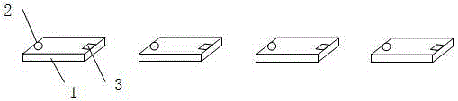
[0029] (1) Such as figure 1 As shown, the lower row of LED chips are arranged, and the LED chips in the lower row are arran...


PUM


Abstract

The invention discloses an LED lamp filament illuminating strip and a preparation method therefor. The illuminating strip comprises LED chips in upper and lower rows, wherein all LED chips in the lower row are distributed at intervals, and all LED chips in the upper row are respectively connected between two adjacent LED chips in the lower row in a lap joint manner. The illuminating surfaces of the LED chips in the upper and lower rows are opposite to each other. The positive and negative electrodes of all LED chips in the upper row are respectively welded with the negative and positive electrodes of two adjacent LED chips, in lap joint connection with the LED chips in the upper row, in the lower row. The preparation method comprises the steps: coating solder paste on the positive and negative electrodes of all LED chips in the lower row; heating the solder paste and enabling the solder paste to be melted, welding the corresponding electrodes, coating the front and back surfaces of chip strips in series connection with fluorescent glue, and solidifying the fluorescent glue. The illuminating strip employs the chips which are not overlapped with each other, and the illuminating surfaces of the chips are arranged oppositely, thereby improving the light-emitting uniformity and facilitating heat dissipation. The wire crossing and tandem among chips is avoided, the packaging cost is reduced, and the yield of finished products is improved.

Description

Technical field [0001] The invention relates to an LED filament light-emitting strip and a preparation method thereof, and belongs to the technical field of semiconductor light-emitting device manufacturing. Background technique [0002] Light-emitting diodes (LEDs) have achieved great development because of their constant current drive, energy saving, environmental protection, small size, low power consumption, and long service life. Compared with traditional incandescent lamps, LED luminescence is difficult to directly replace traditional incandescent lamps due to its point light source and directional characteristics. Therefore, people now make LED chips into filament strips through the packaging process and connect them to current power supplies. Then it can emit light at all angles like a tungsten lamp. Among them, the LEDs in the LED filament lamp are usually fixed together in series or parallel, or a combination of series and parallel, connected by wires, and then assembl...

Claims


Application Information

Patent Timeline
Patent Type & Authority Applications(China)
IPC IPC(8): H01L33/62H01L25/075
CPCH01L25/0753H01L33/62
Inventor 于峰彭璐夏伟徐现刚
Owner SHANDONG INSPUR HUAGUANG OPTOELECTRONICS
Why Eureka
Try Eureka