Photovoltaic power generation element and manufacturing method thereof

A photovoltaic power generation and component technology, applied in the field of solar cells, can solve the problems of characteristic degradation, increase of internal defects of the crystal, difficulty in ensuring electrical and optical characteristics at the same time, and achieve the effect of series resistance

Inactive Publication Date: 2017-03-29
MITSUBISHI ELECTRIC CORP
View PDF10 Cites 0 Cited by
  • Summary
  • Abstract
  • Description
  • Claims
  • Application Information

AI Technical Summary

Problems solved by technology

[0011] However, if this method is applied to a crystalline solar cell, the power generation layer is a crystalline substrate, and if insulating fine particles are dispersed inside, the number of defects inside the crystal increases and the characteristics deteriorate significantly.
In addition, even if it is arranged at the interface of a certain layer of a crystalline silicon solar cell with a conventional structure, the particles themselves have insulating properties, and it is difficult to ensure both electrical and optical properties.

Method used


Image

  • Photovoltaic power generation element and manufacturing method thereof
  • Photovoltaic power generation element and manufacturing method thereof
  • Photovoltaic power generation element and manufacturing method thereof

Examples


Embodiment approach 1

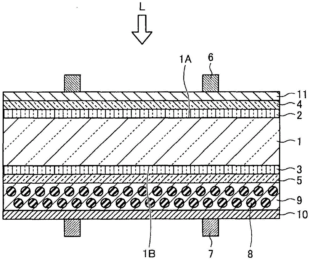
[0035] The photovoltaic power generation element according to Embodiment 1 has a structure in which a crystalline semiconductor substrate of the first conductivity type is used, and an amorphous semiconductor thin film of the second conductivity type different from the semiconductor substrate is provided on the first main surface of the semiconductor substrate. , between the semiconductor substrate and the second conductive type amorphous semiconductor thin film, there is a first amorphous semiconductor thin film that is substantially intrinsic, and on the second main surface of the substrate, there is a first conductive type of the same conductivity type as that of the substrate. The amorphous semiconductor thin film has a substantially intrinsic second amorphous semiconductor thin film between the substrate and the first conductive type amorphous semiconductor thin film, and a transparent semiconductor thin film is provided on the second conductive type amorphous semiconductor...

Embodiment approach 2

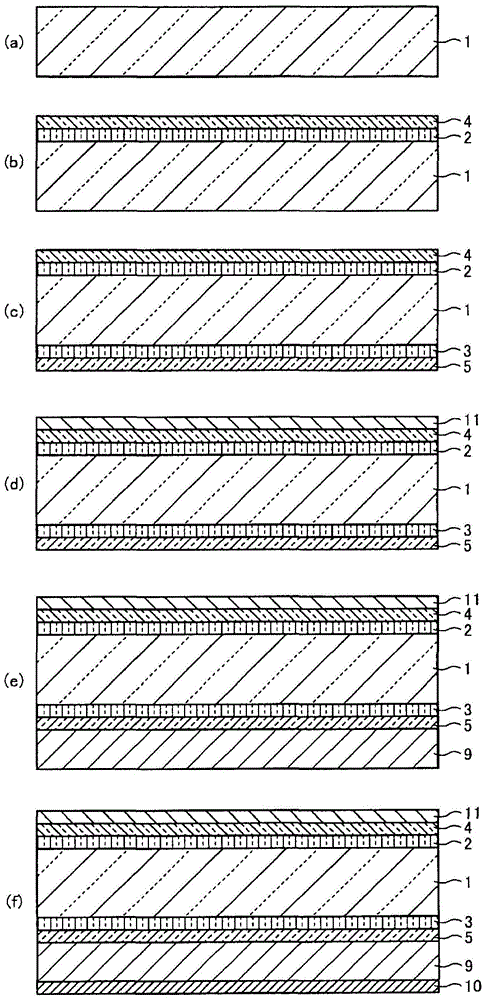
[0063] Figure 5 is a cross-sectional view showing the photovoltaic power generation element of Embodiment 2, Figure 6 is a flowchart showing the manufacturing process of the photovoltaic power generation element, Figure 7 is a process sectional view. In Embodiment 1 above, the method of forming the first and second indium oxide layers 9 and 10 by directly coating and firing on the n-type amorphous silicon layer 5 is used, but in this embodiment, the A method of preventing deterioration of the semiconductor layer through the firing process. That is, in this embodiment, it is a photovoltaic power generation element in which a metal substrate 7S is used as a collector electrode on the back side, and the second indium oxide layer 10 and the second indium oxide layer 10 are sequentially formed on the metal substrate 7S. The first indium oxide layer 9 is formed by being directly bonded to the n-type single crystal silicon substrate 1 formed with layers up to the n-type amorpho...

Embodiment approach 3

[0072] Figure 8It is a sectional view showing the structure of the photovoltaic power generation element according to Embodiment 3 of the present invention. The light L used for power generation enters from the side of the translucent conductive film 11 . The photovoltaic power generation element of Embodiment 3 is characterized in that a third conductive semiconductor film is provided between the first conductivity type amorphous semiconductor thin film and the first conductive semiconductor film in the photovoltaic power generation element of Embodiment 1 above, and The carrier concentration of the third conductive semiconductor film is higher than that of the first conductive semiconductor film.

[0073] Here, if Figure 8 As shown, the third conductive semiconductor thin film is the third indium oxide layer 13, and the carrier concentration is 1×10 19 cm -3 Above and 5×10 20 cm -3 In the range below, the thickness is preferably not less than 1 nm and not more than 1...


PUM


Abstract

This photovoltaic element is provided with: an amorphous semiconductor film of a first conductivity type (an n-type amorphous silicon layer (5)) on a surface of an n-type single crystal silicon substrate (1) serving as a semiconductor substrate, said surface being on the reverse side of the light incident surface; a first conductive semiconductor film (a first indium oxide layer (9)) having a low carrier concentration on the amorphous semiconductor; and a second conductive semiconductor film (a second indium oxide layer (10)) having a high carrier concentration on the first conductive semiconductor film. Insulating fine particles (8) are contained in the first conductive semiconductor film having a low carrier concentration. Consequently, adsorption at the conductive semiconductor films does not occur and no loss is caused even if light is scattered and the optical path length is increased. In addition, a good balance is achieved between suppression of infrared absorption and increase of the optical path length by means of effective scattering, so that a high conversion efficiency can be achieved without causing deterioration in the electrical characteristics even if a thin semiconductor substrate of 100 μm or less is used.

Description

technical field [0001] The present invention relates to a photovoltaic power generation element and a manufacturing method thereof, and particularly to a photovoltaic power generation element such as a solar cell formed using a heterojunction of an amorphous semiconductor and a crystalline semiconductor, and a manufacturing method thereof. Background technique [0002] Conventionally, crystalline solar cells using crystalline semiconductor substrates, particularly crystalline silicon solar cells using crystalline silicon substrates, have high photoelectric conversion efficiency and have been widely used in practical use. Among them, among heterojunction solar cells using an amorphous or microcrystalline semiconductor thin film as a conductive thin film, a solar cell having an intrinsic semiconductor thin film between the conductive thin film and a crystalline substrate has been developed. With regard to this solar cell, the intrinsic semiconductor film between the crystal su...

Claims


Application Information

Patent Timeline
Patent Type & Authority Patents(China)
IPC IPC(8): H01L31/0747H01L31/054H01L31/0224
CPCH01L31/0747H01L31/022425H01L31/056Y02E10/52
Inventor 绵引达郎
Owner MITSUBISHI ELECTRIC CORP
Why Eureka
Try Eureka