Manufacturing method of high-density inductor

A manufacturing method, high-density technology, applied in the direction of circuits, electrical components, electrical solid devices, etc., can solve the problems of high packaging cost, low inductance value, limited process compatibility, etc., to improve product performance and simple process steps Effect

Inactive Publication Date: 2015-12-23
SHANGHAI INST OF MICROSYSTEM & INFORMATION TECH CHINESE ACAD OF SCI
View PDF8 Cites 5 Cited by
  • Summary
  • Abstract
  • Description
  • Claims
  • Application Information

AI Technical Summary

Problems solved by technology

Compared with the integrated magnetic material inductor in the package, the manufacturing of the inductor on silicon is limited by the compatibility of the silicon process, and the thickness of the inductor coil and the magnetic film is limited. The typical structural cross-section is shown in the figure. The inductance value of the inductor Low, small saturation current, high DC resistance
[0004] Due to the high cost of traditional packaging, it cannot fully reflect the superiority of embedded passive devices

Method used


Image

  • Manufacturing method of high-density inductor
  • Manufacturing method of high-density inductor
  • Manufacturing method of high-density inductor

Examples


Embodiment Construction

[0030] The implementation of the present invention will be illustrated by specific specific examples below, and those skilled in the art can easily understand other advantages and effects of the present invention from the contents disclosed in this specification.

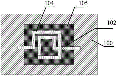
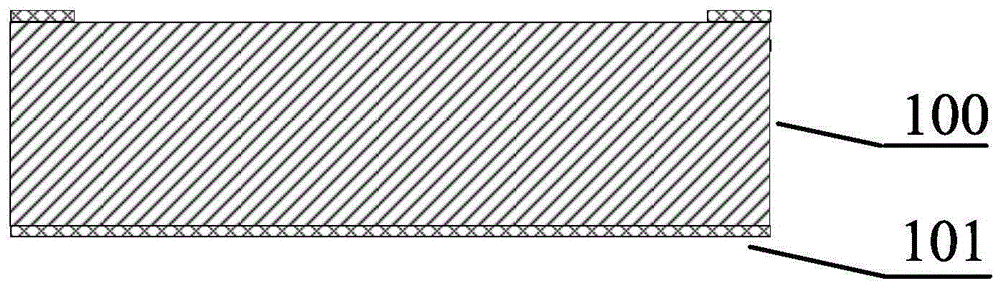
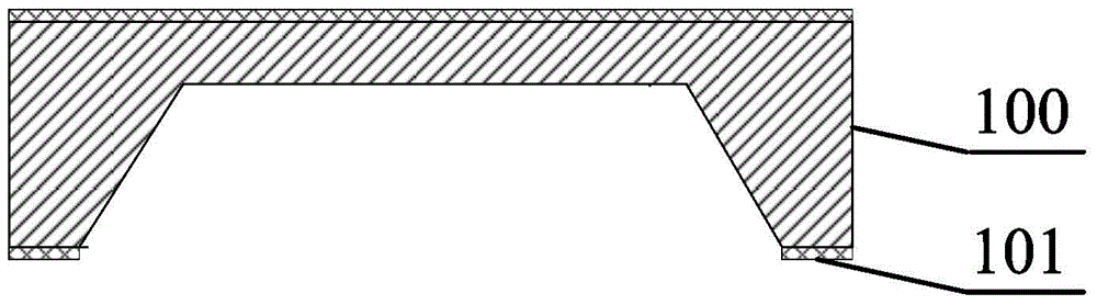
[0031] see Figure 1 to Figure 8 . It should be noted that the structures, proportions, sizes, etc. shown in the drawings attached to this specification are only used to match the content disclosed in the specification, for those who are familiar with this technology to understand and read, and are not used to limit the implementation of the present invention. Limiting conditions, so there is no technical substantive meaning, any modification of structure, change of proportional relationship or adjustment of size, without affecting the effect and purpose of the present invention, should still fall within the scope of the present invention. The disclosed technical content must be within the scope covered. At the sa...


PUM

PropertyMeasurementUnit
particle sizeaaaaaaaaaa

Abstract

The invention provides a manufacturing method of a high-density inductor. The manufacturing method comprises the steps: as follows: (A) a corrosion window is formed in the back surface of a silicon substrate after mask layers are deposited on the front surface and the back surface of the silicon substrate; (B) a deep pit structure located in the silicon substrate is formed along the corrosion window; (C) a first metal pattern layer is formed on the mask layer on the front surface of the silicon substrate; (D) a dielectric layer is subjected to spin-coating on the structure obtained in the step (C) and is patterned, so as to form a through hole which exposes partial first metal pattern layer; (E) a second metal pattern layer is formed on the structure obtained in the step (D), so that partial second metal pattern layer contacts the first metal pattern layer through the through hole; and (F) a composite magnetic material of benzocyclobutene (BCB) and magnetic powder is filled into the deep pit structure and is cured. The silicon substrate below a planar coil inductor is hollowed out by a dry and wet hybrid method corrosion technology; and the composite magnetic material is filled into the deep pit in the back surface of the inductor through a screen-printing technology. Therefore, the inductance value is improved.

Description

technical field [0001] The invention relates to wafer-level integration of passive devices, in particular to a manufacturing method of high-density inductance. Background technique [0002] Magnetic devices such as inductive devices and their power transformers, filters, DC / DC converters, amplifiers, oscillators and tuners are essential and important components in electronic circuits. One of the keys of light weight and high performance, especially the miniaturized DC / DC converter composed of magnetic thin film micro-inductance devices will be widely used in various portable electronic products. Therefore, the market has put forward a very urgent demand for the development of high-power miniaturized integrated inductor devices. [0003] Compared with the traditional discrete magnetic core inductors, in order to meet the needs of system integration, micro-inductors with integrated magnetic materials are mainly divided into two categories based on CMOS technology and packagin...

Claims


Application Information

Patent Timeline
Patent Type & Authority Applications(China)
IPC IPC(8): H01L49/02H01L23/64
Inventor 郑涛罗乐徐高卫韩梅
Owner SHANGHAI INST OF MICROSYSTEM & INFORMATION TECH CHINESE ACAD OF SCI
Why Eureka
Try Eureka