Solid-state imaging device, method of manufacturing solid-state imaging device, and electronic apparatus

a solid-state imaging and imaging device technology, applied in the direction of radioation control devices, television system scanning details, television systems, etc., can solve the problems of increasing wiring resistance, reducing and reducing so as to reduce the number of manufacturing steps and reduce the number of pixel sizes. , the effect of ensuring the reliability of solid-state imaging devices

Inactive Publication Date: 2012-11-27
SONY SEMICON SOLUTIONS CORP
View PDF5 Cites 2 Cited by
  • Summary
  • Abstract
  • Description
  • Claims
  • Application Information

AI Technical Summary

Benefits of technology

[0017]In the solid-state imaging device having two horizontal transfer registers, the transfer portion between the two horizontal transfer registers is employed, as described above, because of the necessity of transferring the signal charges between the plural horizontal transfer registers. This increases the number of layers of the transfer electrodes to be formed in the solid-state imaging device.
[0020]Moreover, when the polysilicon electrodes are formed in three layers, the oxide film 113 between the polysilicon electrodes of the first and third layers is necessarily formed for a longer oxidation time than that taken to form the oxide film 113 between the polysilicon electrodes of the first and second layers or the oxide film 113 between the polysilicon electrodes of the second and third layers. Thus, the oxide film 113 between the polysilicon electrodes of the first and third layers has a larger thickness. From the viewpoint of realizing lower-voltage driving in the CCD solid-state imaging device, it is effective to reduce the thickness of the interlayer insulating film that is made of the oxide film 113. The interlayer insulating film having a larger thickness may impair transfer of the signal charges.
[0021]In the state of the art described above, there is a need for a solid-state imaging device which can reduce the number of manufacturing steps, which is adaptable for further miniaturization of a device element, and which can ensure lower-voltage driving. There is also a need for a method of manufacturing the solid-state imaging device and an electronic apparatus including the solid-state imaging device.
[0038]With the solid-state imaging device according to the embodiment of the present invention, a smaller pixel size can be realized and lower-voltage driving can be ensured. Also, with the method of manufacturing the solid-state imaging device according to the other embodiment of the present invention, the number of manufacturing steps can be reduced. Further, with the electronic apparatus according to the still other embodiment of the present invention, the electronic apparatus can be driven at a lower voltage by using the solid-state imaging device which ensures the lower-voltage driving.

Problems solved by technology

However, when the width of the polysilicon electrode having the reduced size is further narrowed during the manufacturing process, problems may arise in points of, for example, increasing wiring resistance and causing a line break.
Accordingly, reliability of the solid-state imaging device is not ensured.
For that reason, the solid-state imaging device including the three layers of the polysilicon electrodes has a demerit of a difficulty in realizing further miniaturization of the device element.
The interlayer insulating film having a larger thickness may impair transfer of the signal charges.

Method used


Image

  • Solid-state imaging device, method of manufacturing solid-state imaging device, and electronic apparatus
  • Solid-state imaging device, method of manufacturing solid-state imaging device, and electronic apparatus
  • Solid-state imaging device, method of manufacturing solid-state imaging device, and electronic apparatus

Examples


Embodiment Construction

[0049]Embodiments of the present invention will be described below with reference to FIGS. 1 to 7.

[Overall Construction of Solid-State Imaging Device]

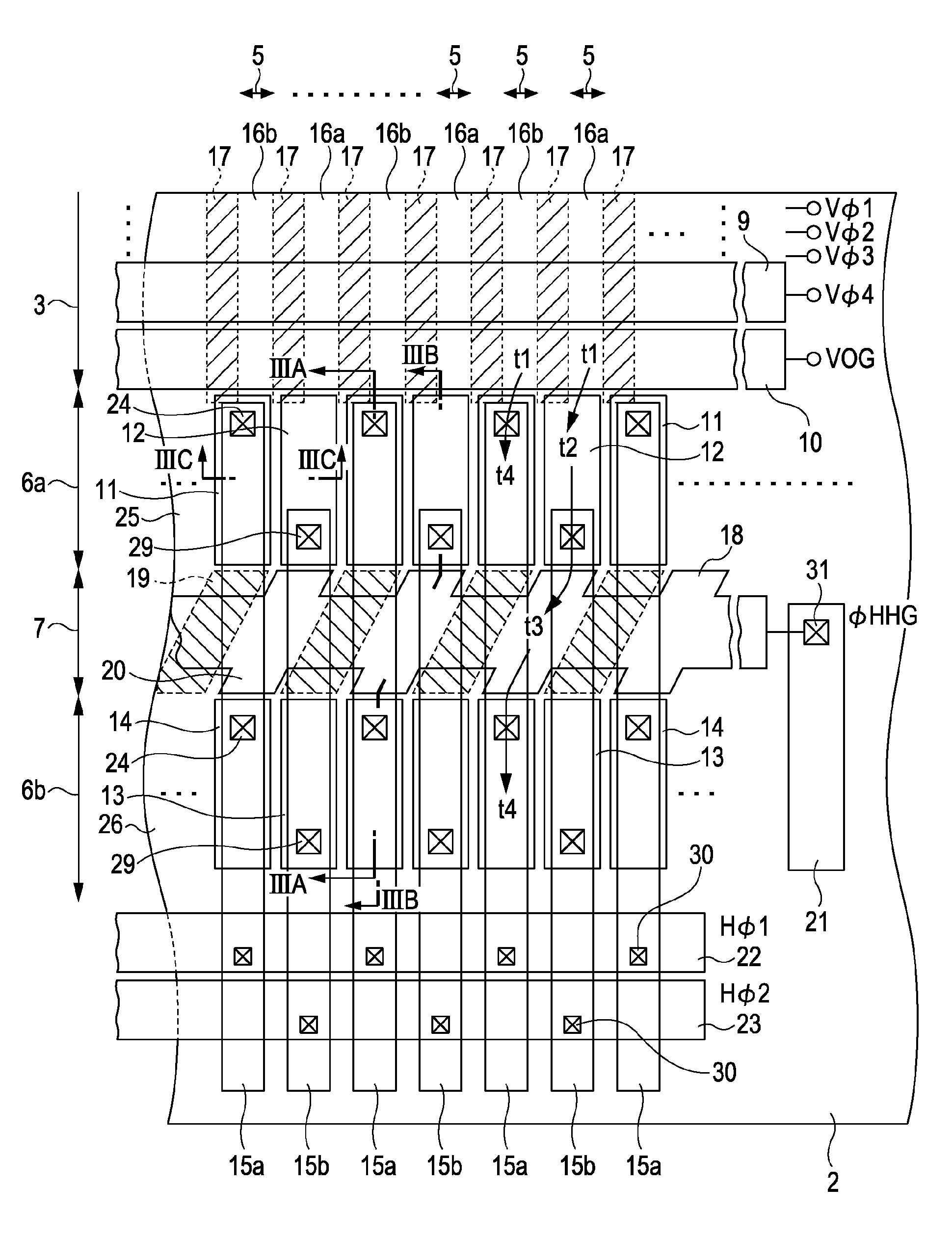
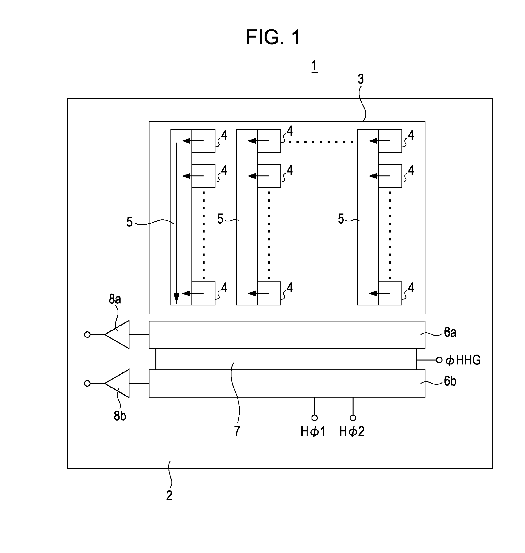
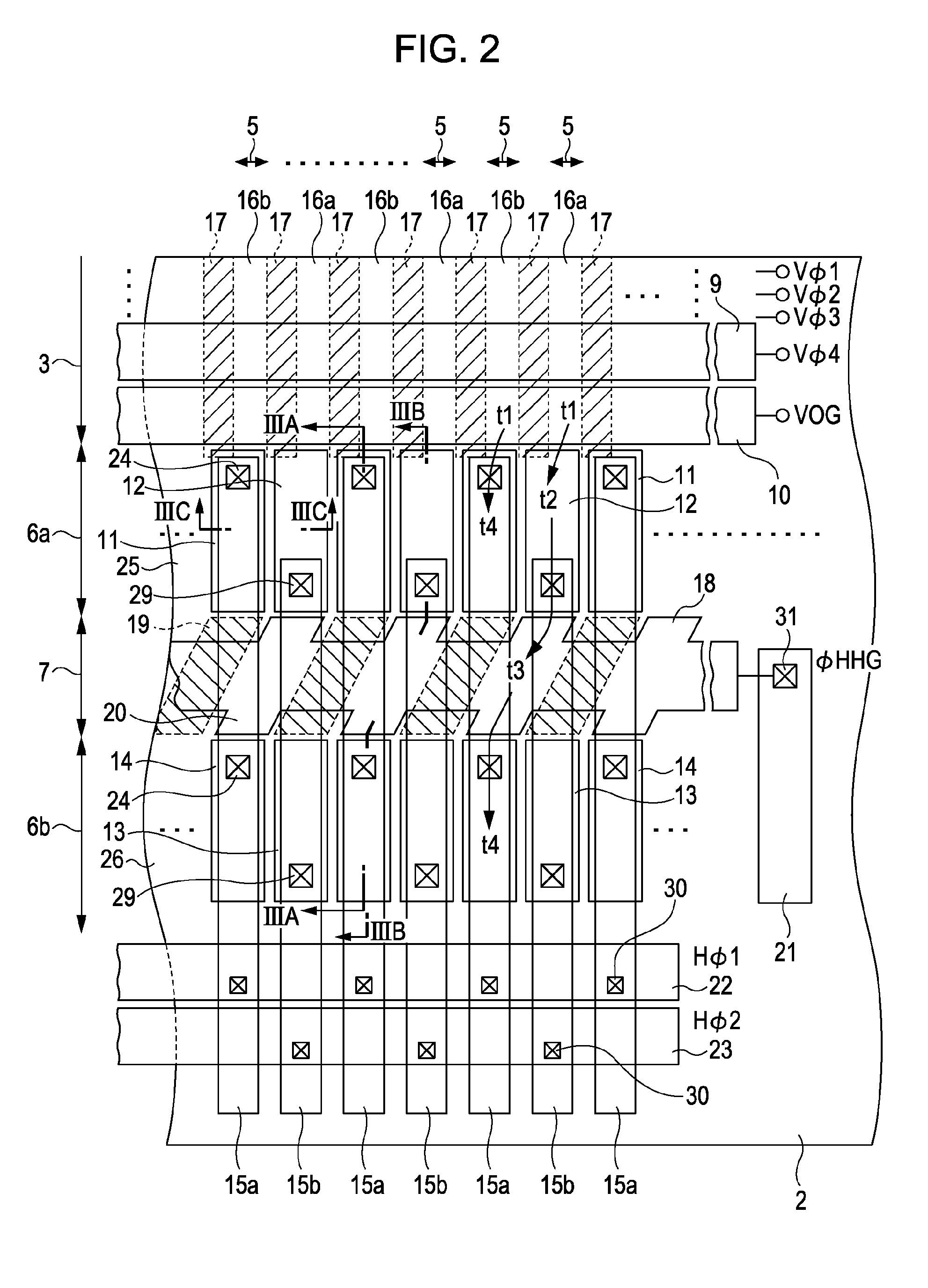
[0050]FIG. 1 is a block diagram illustrating an overall construction of a CCD solid-state imaging device according to the embodiment of the present invention.

[0051]As illustrated in FIG. 1, a CCD solid-state imaging device 1 according to the embodiment includes a plurality of light receiving sensors 4, a plurality of vertical transfer registers 5 each having the CCD structure, and first and second horizontal transfer registers 6a and 6b each having the CCD structure, which are formed in and on a substrate 2. A pixel section 3 is formed by the light receiving sensors 4 and the vertical transfer registers 5. The CCD solid-state imaging device 1 further includes a horizontal-to-horizontal transfer portion (hereinafter referred to as an “H-H transfer portion”) 7 formed between the first and second horizontal transfer registers 6a and 6b, a...


PUM


Abstract

A solid-state imaging device includes a pixel section including light receiving sensors, horizontally spaced vertical transfer registers including vertical transfer channel regions and vertical transfer electrodes formed above the vertical transfer channel regions, vertically spaced horizontal transfer registers each including a horizontal transfer channel region and horizontal transfer electrodes formed side by side in a horizontal direction above the horizontal transfer channel region and formed in the same layer as the vertical transfer electrodes, and a horizontal-to-horizontal transfer portion formed between adjacent two of the horizontal transfer registers and including a horizontal-to-horizontal transfer channel region interconnecting respective parts of the horizontal transfer channel regions positioned under the horizontal transfer electrodes to which the transfer drive pulses having different phases are applied, and a horizontal-to-horizontal transfer electrode formed above the horizontal-to-horizontal transfer channel region in the same layer as both the vertical transfer electrodes and the horizontal transfer electrodes.

Description

BACKGROUND OF THE INVENTION[0001]1. Field of the Invention[0002]The present invention relates to a solid-state imaging device of, e.g., CCD (Charge Coupled Device) type, a method of manufacturing the solid-state imaging device, and an electronic apparatus including the solid-state imaging device.[0003]2. Description of the Related Art[0004]As one example of solid-state imaging devices, there is a device employing a charge coupled device (CCD). In the CCD solid-state imaging device, a plurality of light receiving sensors are arrayed in a two-dimensional matrix pattern and are each made of a photodiode (PD), i.e., a photoelectric transducer for generating and accumulating signal charges that correspond to the amount of light received by the photoelectric transducer. The signal charges are generated and accumulated based on light signals received from a subject (i.e., an object of shooting), which enters the photodiodes of the plural light receiving sensors. The signal charges are tran...

Claims


Application Information

Patent Timeline
Patent Type & Authority Patents(United States)
IPC IPC(8): H04N5/335H04N3/14H01L27/148H04N5/341H04N5/369H04N5/372
CPCH01L27/14831H01L27/146
Inventor KANBE, HIDEO
Owner SONY SEMICON SOLUTIONS CORP
Why Eureka
Try Eureka