Flip-chip LED chip preparation method

A LED chip and flip-chip technology, which is applied in the direction of electrical components, electric solid devices, circuits, etc., can solve the problems of difficult packaging and low voltage, and achieve the effects of uniform current distribution, low voltage, and high brightness

Inactive Publication Date: 2018-06-01
ENRAYTEK OPTOELECTRONICS
View PDF3 Cites 0 Cited by
  • Summary
  • Abstract
  • Description
  • Claims
  • Application Information

AI Technical Summary

Problems solved by technology

[0006] The purpose of the present invention is to provide a method for preparing flip-chip LED chips, which has the advantages of uniform current distribution, low voltage, high brightness, and easy packaging, and overcomes the problems of packaging difficulties in the prior art.

Method used


Image

  • Flip-chip LED chip preparation method
  • Flip-chip LED chip preparation method
  • Flip-chip LED chip preparation method

Examples


Embodiment Construction

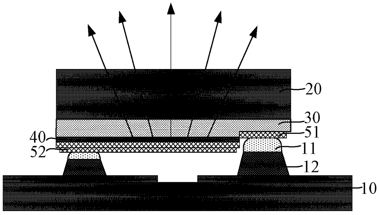
[0030] The method for preparing flip-chip LED chips of the present invention will be described in more detail below in conjunction with schematic diagrams, wherein a preferred embodiment of the present invention is shown, and it should be understood that those skilled in the art can modify the present invention described here, while still implementing the present invention. beneficial effect. Therefore, the following description should be understood as the broad knowledge of those skilled in the art, but not as a limitation of the present invention.

[0031] In the interest of clarity, not all features of an actual implementation are described. In the following description, well-known functions and constructions are not described in detail since they would obscure the invention with unnecessary detail. It should be appreciated that in the development of any actual embodiment, numerous implementation details must be worked out to achieve the developer's specific goals, such as...


PUM

PropertyMeasurementUnit
thicknessaaaaaaaaaa
thicknessaaaaaaaaaa
transmittivityaaaaaaaaaa

Abstract

The present invention proposes a method for preparing a flip-chip LED chip, which uses a layer of isolation layer for isolation, and then forms a bonded P electrode and a bonded N electrode after etching. The flip-chip LED chip has the advantages of uniformity, low voltage, and high brightness. At the same time, since the formed bonding P electrode and bonding N electrode are located on the same plane, there is no need to form a metal chip on the heat dissipation substrate when it is packaged on the heat dissipation substrate. Bumps can be directly packaged on the surface of a flat heat dissipation substrate. Furthermore, the N electrodes can be widely distributed in the form of fingers or rings. On the premise of ensuring uniform current distribution, the etching area is greatly reduced and a larger light-emitting area is retained; the eutectic welding area of ​​flip-chip LED chips It is much larger than the flip-chip LED chip packaged by metal bumps in the prior art, and the heat conduction area is increased, so that it is more conducive to the heat conduction of the flip-chip LED chip.

Description

technical field [0001] The invention relates to the field of LED manufacturing, in particular to a method for preparing a flip-chip LED chip. Background technique [0002] In the traditional front-mounted structure LED (light-emitting diode) chip, P-type GaN is difficult to dope, resulting in low hole carrier concentration and difficulty in growing thick, resulting in difficult current diffusion. At present, it is generally used to prepare ultra-thin metal films or ITO on the surface of P-type GaN. The thin-film approach allows the current to spread evenly. However, the metal thin film electrode layer has to absorb part of the light to reduce the light extraction efficiency. If its thickness is reduced, it will in turn limit the current diffusion layer to achieve uniform and reliable current diffusion on the surface of the P-type GaN layer. Although the light transmittance of ITO is as high as 90%, the electrical conductivity is not as good as that of metal, and the diffusi...

Claims


Application Information

Patent Timeline
Patent Type & Authority Patents(China)
IPC IPC(8): H01L33/00H01L33/38H01L33/64
CPCH01L2224/14H01L2224/16225
Inventor 李智勇徐慧文张宇李起鸣
Owner ENRAYTEK OPTOELECTRONICS
Why Eureka
Try Eureka