Planar VDMOS device and manufacturing method thereof

A manufacturing method and planar technology, which is applied in semiconductor/solid-state device manufacturing, semiconductor devices, electrical components, etc., can solve the problems affecting the dynamic characteristics of VDMOS switches, limited improvement effects, and affecting the metal filling of contact holes, etc., to achieve good switches Effects of dynamic characteristics, reduced capacitance, and increased distance

Active Publication Date: 2016-01-13
FOUNDER MICROELECTRONICS INT
View PDF4 Cites 4 Cited by
  • Summary
  • Abstract
  • Description
  • Claims
  • Application Information

AI Technical Summary

Problems solved by technology

In the structure of planar VDMOS, the capacitance between gate and source is mainly caused by the parasitic capacitance formed between the gate polysilicon layer and the source metal layer, which will affect the switching dynamic characteristics of VDMOS
[0004] In order to reduce the gate-source capacitance value of planar VDMOS, there are currently two main methods. The first method is to reduce the capacitance value by increasing the thickness of the dielectric layer. However, due to the loose texture of the dielectric layer, a thicker dielectric lay

Method used


Image

  • Planar VDMOS device and manufacturing method thereof
  • Planar VDMOS device and manufacturing method thereof
  • Planar VDMOS device and manufacturing method thereof

Examples


Embodiment Construction

[0033] The present invention will be further described below in conjunction with the accompanying drawings and specific embodiments.

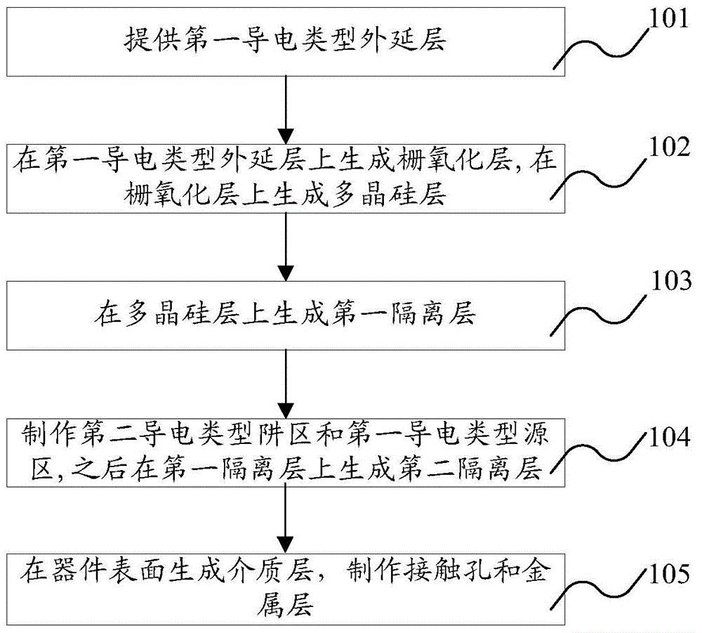
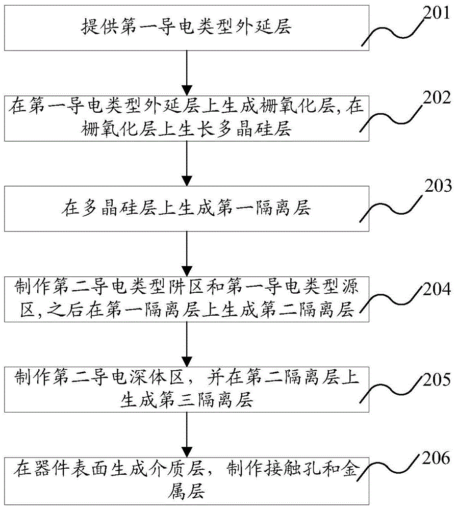
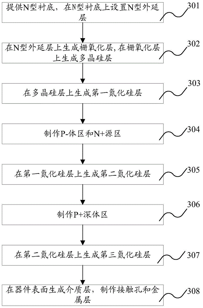
[0034] figure 1 The process flow of a method for manufacturing a planar VDMOS device disclosed in the present invention specifically includes the following steps:

[0035] Step 101: providing a first conductivity type epitaxial layer;

[0036] In this step, a substrate of the first conductivity type can be provided first, and an epitaxial layer of the first conductivity type is formed on the substrate of the first conductivity type. The substrate of the first conductivity type can be an N-type substrate or a P-type substrate. Bottom, when the substrate of the first conductivity type is an N-type substrate, the first conductive epitaxial layer disposed on the N-type substrate is an N-type epitaxial layer; when the substrate of the first conductivity type is a P-type substrate At the bottom, the first conductive epitaxial layer disposed on the ...


PUM


Abstract

The invention discloses a planar VDMOS device and a manufacturing method thereof. The method comprises the steps as follows: providing a first conductivity type substrate, and arranging a first conductivity type epitaxial layer on the first conductivity type substrate; generating a gate oxide layer on the first conductivity type epitaxial layer, and generating a polycrystalline silicon layer on the gate oxide layer; generating a first isolation layer on the polycrystalline silicon layer; making a second conductivity type well region and a first conductivity type source region; and generating a dielectric layer, making a contact hole and a metal layer, and generating a second isolation layer on the first generation layer, wherein the first conductivity type and the second conductivity type are opposite. By growing more dense isolation layers between the gate polycrystalline silicon layer and the source metal layer, the spacing between the gate and source plates is increased, and the gate capacitance and source capacitance of the planar VDMOS device are reduced.

Description

technical field [0001] The invention relates to the field of semiconductor chips, in particular to a planar VDMOS device and a manufacturing method thereof. Background technique [0002] Vertical double diffused field effect transistor (VDMOS) is a power device, its drain and source poles are on both sides of the device, so that the current flows vertically inside the device, increasing the current density, improving the rated current, and the on-resistance per unit area Also smaller, it is a very versatile power device. The most important performance parameter of VDMOS is the operating loss, which can be divided into three parts: conduction loss, cut-off loss and switching loss. The conduction loss is determined by the conduction resistance, the cut-off loss is affected by the reverse leakage current, and the switching loss refers to the loss caused by the charging and discharging of parasitic capacitance during the switching process of the device. It is of great signific...

Claims


Application Information

Patent Timeline
IPC IPC(8): H01L21/336H01L29/78H01L29/06
Inventor 马万里
Owner FOUNDER MICROELECTRONICS INT
Why Eureka
Try Eureka