CMOS device including charged punch-through blocking layer for reducing punch-through and manufacturing method thereof

一种穿通阻止层、带电荷的技术,应用在半导体/固态器件制造、电固体器件、电气元件等方向,能够解决难以形成穿通阻止层陡峭分布等问题,达到抑制漏电流的效果

Active Publication Date: 2016-01-13
INST OF MICROELECTRONICS CHINESE ACAD OF SCI
View PDF4 Cites 3 Cited by
  • Summary
  • Abstract
  • Description
  • Claims
  • Application Information

AI Technical Summary

Problems solved by technology

[0004] However, it is difficult in the prior art to form a steep profile of the punch-through stop layer (ie, from almost no doping in the fin to a high doping below the fin)

Method used


Image

  • CMOS device including charged punch-through blocking layer for reducing punch-through and manufacturing method thereof
  • CMOS device including charged punch-through blocking layer for reducing punch-through and manufacturing method thereof
  • CMOS device including charged punch-through blocking layer for reducing punch-through and manufacturing method thereof

Examples


Embodiment Construction

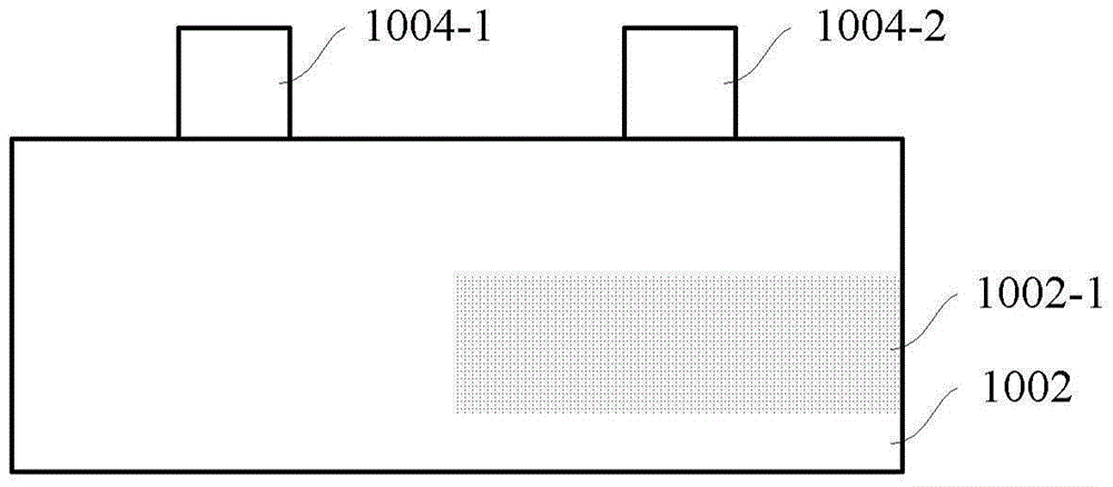
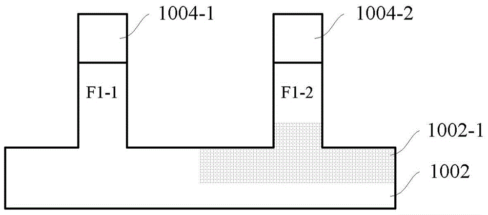
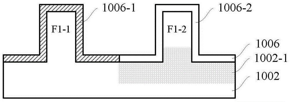
[0015] Hereinafter, embodiments of the present disclosure will be described with reference to the drawings. It should be understood, however, that these descriptions are exemplary only, and are not intended to limit the scope of the present disclosure. Also, in the following description, descriptions of well-known structures and techniques are omitted to avoid unnecessarily obscuring the concepts of the present disclosure.

[0016] Various structural schematic diagrams according to embodiments of the present disclosure are shown in the accompanying drawings. The figures are not drawn to scale, with certain details exaggerated and possibly omitted for clarity of presentation. The shapes of the various regions and layers shown in the figure, as well as their relative sizes and positional relationships are only exemplary, and may deviate due to manufacturing tolerances or technical limitations in practice, and those skilled in the art will Regions / layers with different shapes, ...


PUM


Abstract

The invention discloses a CMOS device including a charged punch-through blocking layer for reducing punch-through and a manufacturing method thereof. According to the embodiment, the CMOS device comprises an n-type device and a p-type device. Each of the n-type device and the p-type device can comprise a fin-shaped structure which is formed on a substrate; an isolation layer which is formed on the substrate, wherein the part of the fin-shaped structure above the isolation layer acts as the fins of the n-type device or the p-type device; the charged punch-through blocking layer which is formed at the side wall of the sub-fin part of the fin-shaped structure; and a gate stack which is formed on the isolation layer and intersected with the fins, wherein the punch-through blocking layer carries net negative charges as for the n-type device, and the punch-through blocking layer carries net positive charges as for the p-type device.

Description

technical field [0001] The present disclosure relates to the field of semiconductors, and more particularly, to a complementary metal-oxide-semiconductor (CMOS) device including a charged punch-through preventing layer to reduce punch-through and a method of manufacturing the same. Background technique [0002] As the size of planar semiconductor devices becomes smaller and smaller, the short channel effect becomes more and more obvious. For this reason, three-dimensional semiconductor devices such as FinFETs (Fin Field Effect Transistors) have been proposed. In general, a FinFET includes a fin formed vertically on a substrate and a gate intersecting the fin. [0003] In particular, in a bulk FinFET (i.e., a FinFET formed on a bulk semiconductor substrate, and more specifically, a fin formed from and thus in contact with the bulk semiconductor substrate), there may be Leakage through the portion of the substrate below the fin, which may also be referred to as punch-through...

Claims


Application Information

Patent Timeline
Patent Type & Authority Applications(China)
IPC IPC(8): H01L27/118H01L27/02H01L21/8238
CPCH01L27/0924H01L21/326H01L21/823807H01L21/823821H01L21/823878H01L29/0649H01L29/1083H01L29/66545
Inventor 朱慧珑魏星
Owner INST OF MICROELECTRONICS CHINESE ACAD OF SCI
Why Eureka
Try Eureka