A method for preventing excessive etching of ICP in a sog-mems chip

An over-etching and chip technology, which is applied in the fields of crafts, decorative arts, and gaseous chemical plating for producing decorative surface effects, to achieve the effects of improving yield, reducing costs, and preventing over-etching

Active Publication Date: 2017-04-05
BEIJING INST OF AEROSPACE CONTROL DEVICES
View PDF3 Cites 2 Cited by
  • Summary
  • Abstract
  • Description
  • Claims
  • Application Information

AI Technical Summary

Problems solved by technology

Through the uniform control of the exposed area width and the accurate monitoring of the etching end point, the problem of ICP over-etching is effectively solved

Method used


Image

  • A method for preventing excessive etching of ICP in a sog-mems chip
  • A method for preventing excessive etching of ICP in a sog-mems chip
  • A method for preventing excessive etching of ICP in a sog-mems chip

Examples


Embodiment 1

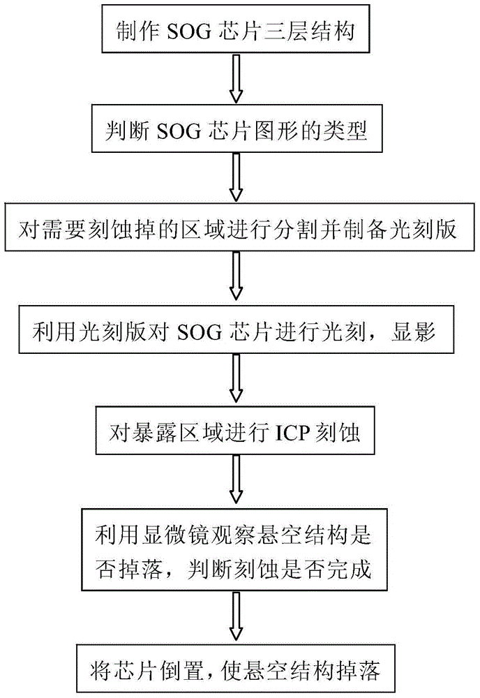
[0033] Embodiment 1: The pattern processing includes etching away a plurality of rectangles and etching through a plurality of linear chips composed of the same line width. Processing flow such as figure 1 shown.

[0034] 1. Preparation of SOG chip.

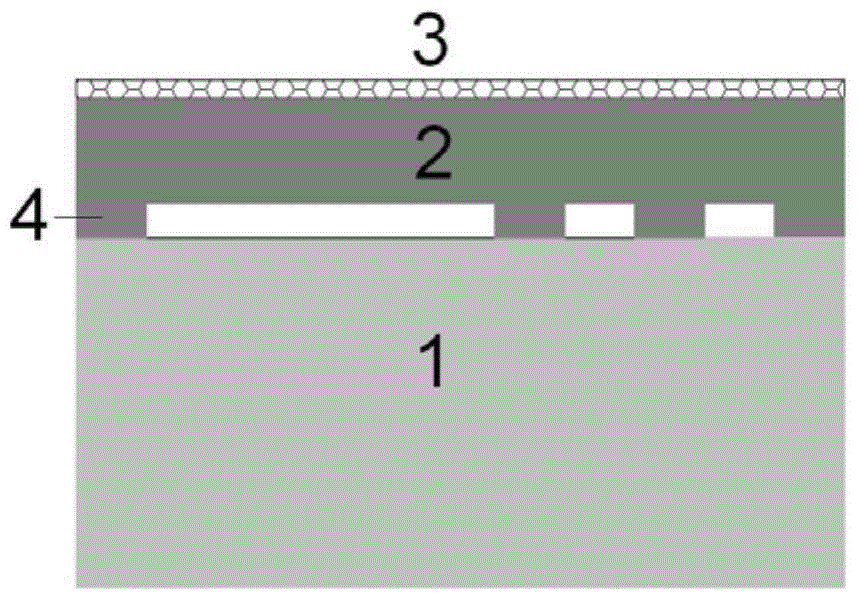
[0035] SOG structure such as figure 2 As shown, it includes a support layer 1, a structure layer 2, and a mask layer 3; the support layer 1 is made of glass material, the structure layer 2 is made of silicon material, and the mask layer 3 is made of photoresist. A plurality of anchor points 4 are etched on the side of the silicon layer facing the glass layer. The height of the anchor points is generally 5-30um. In this example, the height of the anchor points is set to 10um. An isolation groove 5 is formed between every two anchor points 4 The silicon wafer is connected with the glass wafer through the anchor point; the glass layer and the silicon layer are bonded together and the silicon layer is thinned by chemical mechanic...

Embodiment 2

[0058] Embodiment 2: The pattern processing includes etching out multiple rectangles and etching through multiple linear chips composed of different line widths.

[0059] Processing flow such as figure 1 shown.

[0060] 1, the preparation of SOG chip is the same as embodiment one;

[0061] 2. Determine the type of chip graphics.

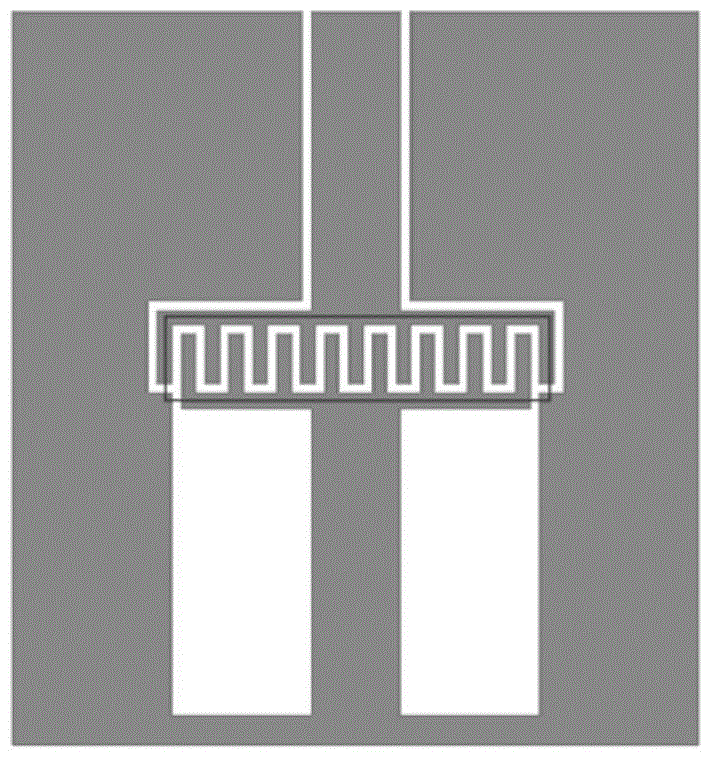
[0062] The pattern of the chip also includes etching away 4 rectangles and etching through 16 lines with different line widths. The schematic diagram of the surface structure is shown in Figure 4(a). The white rectangular area in the figure is the etched area. The minimum side length of the rectangle is 45um. The area in the wire frame is a line shape composed of different line widths. The line width in area a is the smallest, which is 3um, and the line width in area b is The line width in area b is 5um, the line width in area c is 5um, and the line width in area d is the largest, which is 6um. The length of the shortest side of the rectangle is ...

Embodiment 3

[0071] Embodiment three: processing chips of other linear structures

[0072] The linear structure can be H-shaped or other shapes, and the end of the linear structure can be rectangular or arc-shaped. These structures are widely used in MEMS devices.

[0073] All the other steps are the same as in Embodiment 1.


PUM


Abstract

The invention provides a method for preventing ICP excessive etching in an SOG-MEMS chip. For simultaneously etching multiple rectangles and through etching multiple line shapes with the same line width or different line widths, a central non-exposed area (12) is arranged in each rectangle needing to be etched on a photoetching board and forms a to-be-etched exposed area with the middle of the frame, that is, an external non-exposed area (11) of the rectangle, and the width of the to-be-etched exposed area is equal to the line width of the minimum line shape to be through etched; the uniform of the etching strip width is guaranteed, and the problem of an Lag effect in the etching process of the structure with the different strip widths is solved; meanwhile, when etching is completed, the central non-exposed areas (12) fall onto supporting layers (1) under the central non-exposed areas (12), and therefore the fact that etching is completed can be accurately judged. The method has the advantages that seriously excessive etching of the MEMS structure with the different etching strip width in ICP etching can be effectively prevented from being caused.

Description

technical field [0001] The invention relates to a method for preventing excessive etching of ICP in a SOG-MEMS chip. The invention belongs to the field of micro-electromechanical system (MEMS) device processing, especially for dry etching technology for making MEMS devices with a silicon-glass structure. A method for preventing or reducing excessive etching in ICP etching and performing endpoint detection in a SOG-MEMS chip. Background technique [0002] SOG-MEMS structures based on silicon-glass bonding and ICP deep silicon etching are widely used in inertial devices and other sensors. In the process of processing, it is necessary to bond the silicon layer with anchor points to the glass layer first, and the glass layer acts as a support. After thinning the silicon surface to the required thickness, photolithography is performed, and then inductively coupled plasma The bulk (ICP) equipment performs dry etching on the silicon structure layer to complete the release of the s...

Claims


Application Information

Patent Timeline
Patent Type & Authority Patents(China)
IPC IPC(8): B81C1/00
Inventor 梁德春刘福民邢朝洋徐宇新李昌政刘宇
Owner BEIJING INST OF AEROSPACE CONTROL DEVICES
Why Eureka
Try Eureka