

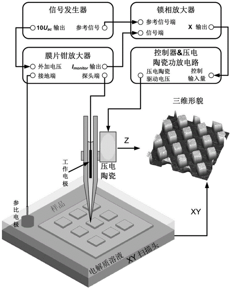
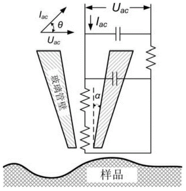
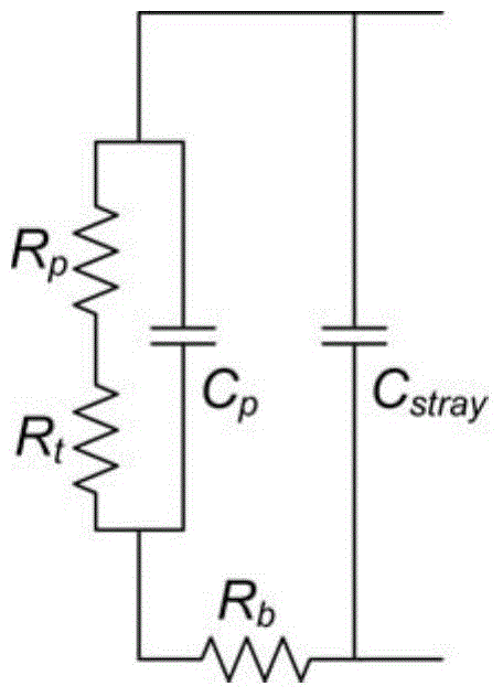
Phase modulation imaging mode scanning device and method of SICM
An imaging mode, phase modulation technology, applied in measurement devices, scanning probe technology, scanning probe microscopy, etc., can solve the problems of slow scanning speed, poor system stability, etc. The effect of speeding up scanning
- Summary
- Abstract
- Description
- Claims
- Application Information
AI Technical Summary
Problems solved by technology
Method used
Image

Examples
Embodiment 1
[0049] 1. Use a standard grid of silicon material (P / N498-000-026, Digital Instruments) with a width of 5μm and a depth of 200nm for AFM calibration as the master, face up, and pour 10:1 PDMS (Sylgard184, DowCorning) The mixture of the main agent and hardener evenly stirred; vacuum for another 20 minutes to make the mixture free of bubbles; then place it on the heating plate (PC-600, Corning) and bake at 70°C for 4-5 hours; finally, after curing The PDMS layer is torn off from the silicon standard grid. At this time, the PDMS surface close to the silicon grid will be imprinted with a fine structure complementary to the grid, thus obtaining a PDMS material grid sample.
[0050] 2. Put the side of the PDMS sample with the imprinted structure facing up, and dip the bottom surface into a Φ35mm petri dish. Use a micropipette to pour phosphate buffer saline (PBS) into the petri dish. The best solution is 2mm above the surface of the PDMS sample;
[0051] 3. The glass tube probe is drawn ...
PUM
 Abstract
Description
Claims
Application Information