Demolding method in nanoimprint technology process

A nano-imprinting and technical technology, applied in the field of micro-nano processing, can solve the problems of tearing and demolding force, deformation of nano-imprinting structure, etc.

CN105319838AInactive Publication Date: 2016-02-10SHANDONG UNIV OF SCI & TECH
1 Cites 5 Cited by

Patent Information

Authority / Receiving Office
CN · China
Patent Type
Applications(China)
Current Assignee / Owner
Publication Date
2016-02-10
Estimated Expiration
Not applicable · inactive patent

Smart Images

  • Figure 1
    Figure 1
Patent Text Reader

Abstract

The invention discloses a demolding method in a nanoimprint technology process. The demolding method comprises the following steps: firstly, coating a substrate with a nanoimprint adhesive material to form an imprint adhesive layer; secondly, pressing a template into the imprint adhesive layer; thirdly, transmitting an ultrasonic wave to the template by an ultrasonic transmitting device at the upper part of the template after the imprint adhesive layer is cured and fixed, so as to assist separation of the template and the imprint adhesive layer; and finally removing the template and finishing the demolding process. Compared with the prior art, the problems that the molded nanoimprint structure is serious in deformation, overlarge in tear force and demolding force and the like due to cohesion force of the template and the adhesive layer in the demolding process of a nanoimprint technology are solved; imprinted pattern transferring and photoetching are completely consistent; the demolding force is effectively reduced; the demolding success rate is greatly improved; and large-scale industrial production is realized.
Need to check novelty before this filing date? Find Prior Art

Description

technical field

[0001] The invention relates to a demoulding method in the process of nano-imprint technology, which belongs to the field of micro-nano processing. Background technique

[0002] Nanoimprint technology was first proposed in the mid-1990s by Professor Stephen Y. Chou of the Nanostructure Lab of Princeton University in the United States, aiming at the disadvantage of the traditional photolithography process being limited by the exposure wavelength and unable to obtain a smaller size. Due to its low cost, high resolution, simple process and other advantages, this technology has attracted extensive attention of researchers from all over the world. At present, it has been successfully demonstrated that nanoimprinting technology can obtain feature structures with a minimum size of 5nm. This technology is widely used in optics, electronics, biology and many other fields, and is known as one of the top ten technologies that can change the world.

[0003] Nanoimprint...

Examples

Embodiment Construction

[0014] The present invention will be further described below in conjunction with the accompanying drawings.

[0015] The present invention takes ultrasonic-assisted demoulding in the process of nano hot embossing technology as a specific embodiment.

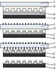
[0016] see figure 1 As shown, an ultrasonic-assisted demoulding method in the process of nano-hot embossing technology, firstly, the nano-imprint polymer is coated on the substrate, heated to melt and soften, and the embossed adhesive layer 3 is formed; then the template 2 Press into the embossed adhesive layer 3; after the embossed adhesive layer 3 is cured and shaped, use the ultrasonic emission device 1 on the upper part of the template 2 to emit ultrasonic waves to the template 2 to assist the separation of the template 2 and the formed embossed adhesive layer 3, and remove the template 2. Complete the demoulding process.

[0017] The ultrasonic waves emitted by the ultrasonic emitting device 1 on the upper part of the temp...