Plasma etching device

An etching device and plasma technology, applied in discharge tubes, electrical components, circuits, etc., can solve the problems of poor control of the profile shape of deep trenches, affecting plasma density, etc., so as to improve process efficiency and product yield Effect

Active Publication Date: 2016-02-17
ADVANCED MICRO FAB EQUIP INC CHINA
View PDF6 Cites 34 Cited by
  • Summary
  • Abstract
  • Description
  • Claims
  • Application Information

AI Technical Summary

Problems solved by technology

[0005] However, although the use of a shadow ring can improve the etching uniformity over the entire substrate in the non-pattern etching process, the shadow ring also affects the plasma density in the edge region at the same time, which will lead to deep trenches in the pattern etching process. poor profile control

Method used


Image

  • Plasma etching device
  • Plasma etching device
  • Plasma etching device

Examples


Embodiment 1

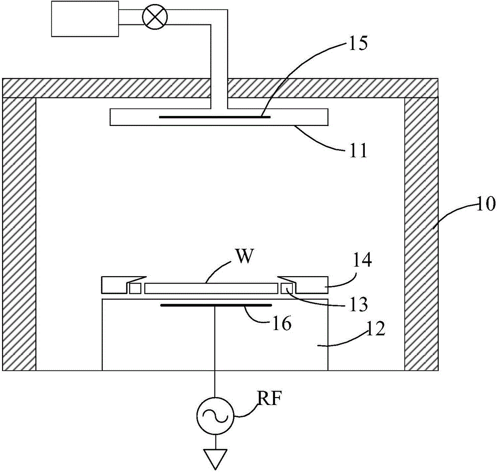
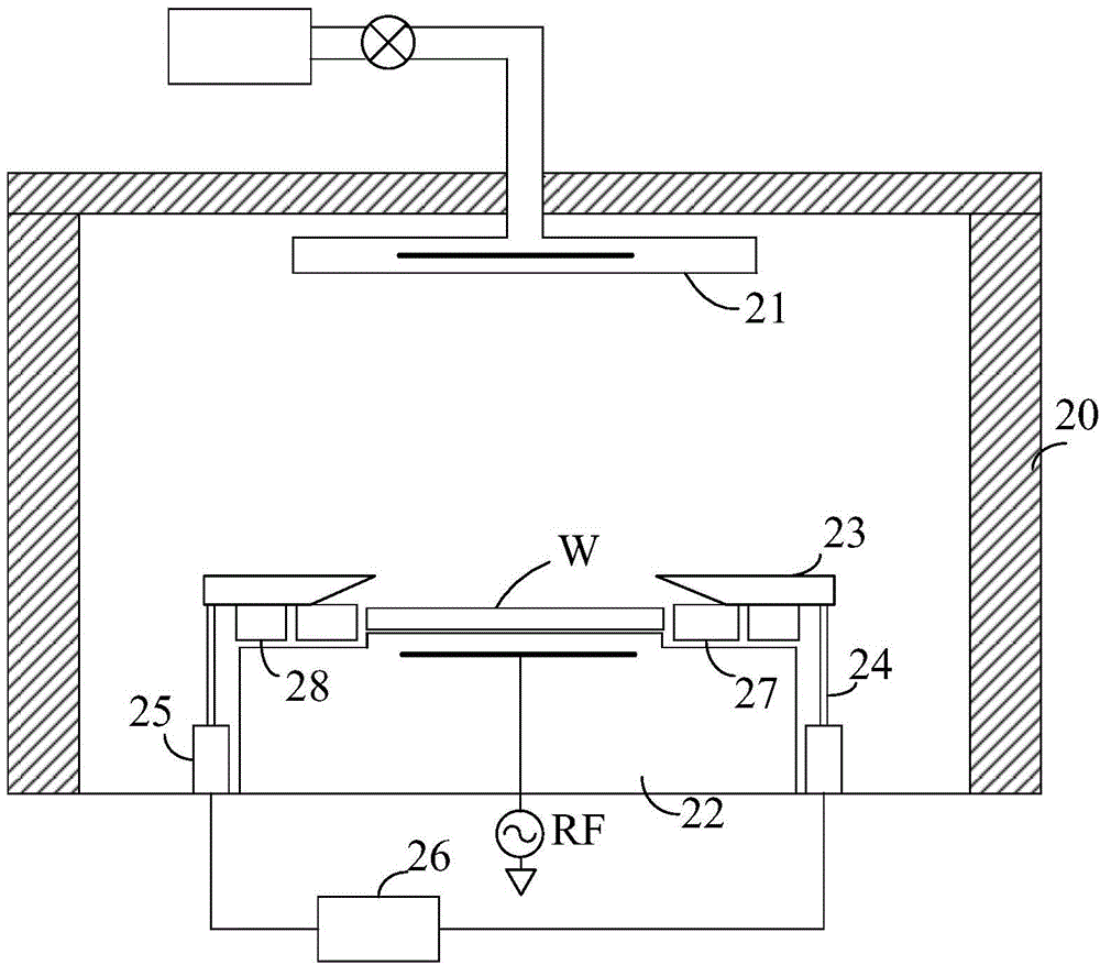
[0030] See Figure 2a and Figure 2b , which is a schematic structural diagram of the plasma etching device in this embodiment. The plasma etching device includes a reaction chamber 20, the top of the reaction chamber 20 is provided with a reaction gas shower head 21, the reaction gas shower head 21 includes an upper electrode, and the bottom of the reaction chamber 20 is provided with a The electrostatic chuck 22 of W, the lower electrode opposite to the upper electrode is arranged in the electrostatic chuck 22 . A radio frequency source RF is applied to the lower electrode to form a radio frequency electric field to ionize the etching gas to generate plasma. A liftable annular shielding member 23 is provided on the outer peripheral side of the substrate. As shown in the figure, the annular shielding member 23 is positioned above the surface of the substrate W in a non-contact manner by the support rod 24 . Preferably, three support rods 24 are evenly distributed along th...

Embodiment 2

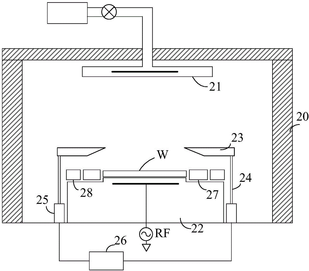
[0034] image 3 It is a structural schematic diagram of another embodiment of the plasma etching device provided by the present invention, which is characterized in that the movable annular shielding member 23 is a gas guide ring. The gas guide ring 23 is disposed above the surface of the substrate W through the support rod 24 in a non-contact manner. Preferably, three support rods 24 are evenly distributed along the circumference of the gas guiding ring 23 , one end of which is fixedly connected to the gas guiding ring 23 , and the other end is connected to the driving unit 25 . The drive unit 25 receives a signal from the control unit 26 to drive the support rod to drive the gas guide ring 23 to move in the vertical direction. Other components in the plasma etching device, such as the electrostatic chuck 22 , the gas shower head 21 , the control unit 26 and the drive unit 25 , can be configured with reference to the foregoing embodiments.

[0035] The gas guide ring 23 its...


PUM


Abstract

The invention discloses a plasma etching device capable of executing a deep groove graph etching process in an in situ mode and executing a free-graphics etching process. The device comprises a reaction chamber. The reaction chamber possesses a static chuck clamping a substrate, a mobile annular shielding component arranged on a periphery side of the substrate and located above the substrate, a driving unit used for driving the annular shielding component to move along a vertical direction and a control unit. When the deep groove graph etching process is about to be performed, the control unit makes the driving unit drive the annular shielding component to be positioned at a first position which is far away from the substrate. When the free-graphics etching process is about to be performed, the control unit makes the driving unit drive the annular shielding component to be positioned at a second position close to the substrate. By using the device, morphology control of high-aspect-ratio structure graph etching and uniformity of free-graphics etching can be effectively improved.

Description

technical field [0001] The invention relates to semiconductor processing equipment, in particular to a plasma etching device. Background technique [0002] With the improvement of integrated circuit integration and the reduction of element line width, the plasma etching (PlasmaEtching) process has been widely used. The plasma etching process is to arrange the electrodes in the reaction chamber of the plasma etching device, provide the etching gas as the reaction gas to the reaction chamber, and form the plasma of the reaction gas in the reaction chamber by applying radio frequency on the electrodes. A dry etching process in which etching is performed by radicals, ions, etc. generated by the plasma. [0003] In recent years, the use of plasma etching process to form high aspect ratio structures, such as TSV technology, is receiving more and more attention and research. The formation of a high aspect ratio structure typically uses a patterned etching process to form a patter...

Claims


Application Information

Patent Timeline
Patent Type & Authority Applications(China)
IPC IPC(8): H01J37/32
Inventor 杨俊李俊良
Owner ADVANCED MICRO FAB EQUIP INC CHINA
Why Eureka
Try Eureka