Semiconductor device and forming method thereof

A semiconductor and device technology, applied in the field of semiconductor devices and their formation, can solve problems such as poor performance and low yield

Active Publication Date: 2016-02-17
SEMICON MFG INT (SHANGHAI) CORP
View PDF5 Cites 5 Cited by
  • Summary
  • Abstract
  • Description
  • Claims
  • Application Information

AI Technical Summary

Problems solved by technology

[0005] However, the existing junction field effect transistors have low yield and poor performance, and it is necessary to improve the structure or manufacturing process of the junction field effect transistor to improve device performance

Method used


Image

  • Semiconductor device and forming method thereof
  • Semiconductor device and forming method thereof
  • Semiconductor device and forming method thereof

Examples


Embodiment Construction

[0033] As mentioned in the background, the existing junction field effect transistors have low yield and poor performance.

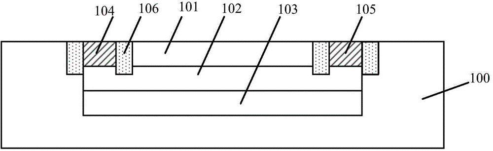
[0034] Please continue to refer figure 1 , the working principle of the junction field effect transistor is: when the top gate doped region 101 and the bottom gate doped region 103 are both grounded, due to the doping in the source region 104, the drain region 105 and the channel region 102 The ions are the same, so the source region 104, the drain region 105 and the channel doped region 102 conduct; when a bias voltage is applied between the top gate doped region 101 and the bottom gate doped region 103, the channel The second doping ions in the channel doping region 102 and the first doping ions in the top gate doping region 101 and the bottom gate doping region 103 are interdiffused, so that the top gate doping region 101, the channel doping region The region 102 and the bottom gate doped region 103 form a depletion layer; moreover, the greater the a...


PUM


Abstract

The invention discloses a semiconductor device and a forming method thereof. The forming method comprises the steps as follows: a substrate is provided; a sacrificial layer is formed on the surface of the substrate; an opening for exposing partial surface of the substrate is formed in the sacrificial layer; a barrier layer is formed at the bottom of the opening; a first semiconductor layer is formed on the surface of the barrier layer and is doped with first ions; a first doped region is formed at the bottom of the first semiconductor layer; the first semiconductor layer is doped with second ions; a second doped region is formed at the top of the first doped region; the second ions and the first ions are different in conductive type; after the first doped region and the second doped region are formed, the sacrificial layer is removed and the surface of the substrate is exposed; after the sacrificial layer is removed, a second semiconductor layer is formed on the surface of the substrate and is doped with the first ions; and a source region and a drain region are formed at two sides of the first doped region and the second doped region respectively. The performance of the formed semiconductor device is improved.

Description

technical field [0001] The invention relates to the technical field of semiconductor manufacturing, in particular to a semiconductor device and a forming method thereof. Background technique [0002] With the rapid development of semiconductor technology, in order to meet the continuous development of various electronic equipment, there are more technical requirements for the power supply of integrated circuits (IC), such as the use of booster (Boostconverter), buckconverter (Buckconverter) And other different voltage regulators are combined to meet the different power requirements of various integrated circuits. Therefore, whether various IC power supplies can be provided has also become one of the important factors in the development of electronic products. [0003] Junction Field Effect Transistor (JFET) is widely used in various devices due to its good performance, especially the junction field effect transistor has good voltage regulation ability, so it can be used as ...

Claims


Application Information

Patent Timeline
Patent Type & Authority Applications(China)
IPC IPC(8): H01L29/808H01L29/06H01L21/337
Inventor 刘金华
Owner SEMICON MFG INT (SHANGHAI) CORP
Why Eureka
Try Eureka