Packaging method

A packaging method and a plastic sealing layer technology, which are applied in the manufacture of electrical components, electrical solid devices, semiconductor/solid devices, etc., can solve problems such as poor reliability and low yield of packaging structures, achieve reliability enhancement, eliminate chip drift problems, The effect of eliminating the warpage of the plastic seal layer

Inactive Publication Date: 2016-02-24
NANTONG FUJITSU MICROELECTRONICS
View PDF8 Cites 24 Cited by
  • Summary
  • Abstract
  • Description
  • Claims
  • Application Information

AI Technical Summary

Problems solved by technology

[0004] However, the reliability of the existing wafer-level packaging technology is poor, and the yield rate of the packaging structure formed by the existing wafer-level packaging technology is low

Method used


Image

  • Packaging method
  • Packaging method
  • Packaging method

Examples


Embodiment Construction

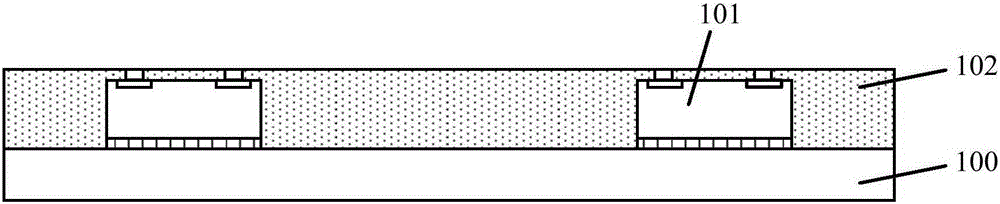
[0038] As mentioned in the background, the reliability of the existing wafer level packaging technology is poor, and the yield rate of the packaging structure formed by the existing wafer level packaging technology is low.

[0039] Please refer to figure 1 , figure 1 It is a schematic cross-sectional structure diagram of an embodiment of a wafer-level packaging structure, including: a carrier 100; several chips 101 fixed on the surface of the carrier 100, the chips 101 including a functional surface; covering the carrier 100 and several chips The plastic sealing layer 102 on the surface of 101. Wherein, after the chip 101 is bonded on the surface of the carrier 100 , the plastic sealing layer 102 is formed through a plastic sealing process such as injection molding or transfer injection, and the plastic sealing layer 102 wraps the chip 101 . After forming the plastic encapsulation layer 102, it also includes: removing the carrier 100 and exposing the functional surface of th...


PUM


Abstract

A packaging method comprises the steps of: providing a carrier plate, wherein the carrier plate comprises a plurality of chip regions and cutting regions arranged between the adjacent chip regions, the carrier plate further comprises a first surface, and a plurality of grooves are formed in the cutting regions in the first surface of the carrier plate; providing chips, wherein each chip comprises a functional surface and a non-functional side surface which are opposite to each other, the surface of each functional surface is provided with bumps, and the bumps protrude out of the functional surfaces; fixing the non-functional side surfaces of the chips with the first surface of the carrier plate in the chip regions; forming a plastic packaging layer on the first surface of the carrier plate and the surfaces of the chips, wherein the plastic packaging layer exposes top part surfaces of the bumps; removing the carrier plate after forming the plastic packaging layer; forming a rewiring structure on the surface of the plastic packaging layer and the functional surfaces of the chips; and cutting the plastic packaging layer and the rewiring structure, so that the plurality of chips are separated from one another, thereby forming an independent packaging structure. The yield and reliability of the formed packaging products are improved.

Description

technical field [0001] The invention relates to the technical field of semiconductor manufacturing, in particular to a packaging method. Background technique [0002] Wafer Level Packaging (WLP for short) technology is a technology that performs packaging and testing on the entire wafer and then cuts it to obtain a single finished chip. The size of the packaged chip is exactly the same as that of the bare chip. Compared with the ceramic leadless chip carrier (CeramicLeadlessChipCarrier) or the organic leadless chip carrier (OrganicLeadlessChipCarrier) and other modes, the wafer level packaging technology has the advantages of being lighter, smaller, shorter, thinner and cheaper. The size of the chip packaged by the wafer-level packaging technology can be highly miniaturized, and the manufacturing cost of the chip will be significantly reduced with the reduction of the chip size and the increase of the wafer size. Wafer-level packaging technology is a technology that can int...

Claims


Application Information

Patent Timeline
Patent Type & Authority Applications(China)
IPC IPC(8): H01L21/56
CPCH01L21/56H01L21/568H01L24/96H01L2224/04105H01L2224/12105H01L2224/19H01L2924/18162H01L2924/3511H01L2924/00012
Inventor 石磊
Owner NANTONG FUJITSU MICROELECTRONICS
Why Eureka
Try Eureka