Check patentability & draft patents in minutes with Patsnap Eureka AI!

A stacked image sensor

An image sensor, stacked technology, applied in the field of stacked image sensors, can solve the problems of low fill factor and low sensitivity of front lighting technology

Active Publication Date: 2018-05-29
SHANGHAI INTEGRATED CIRCUIT RES & DEV CENT +1
View PDF4 Cites 0 Cited by
  • Summary
  • Abstract
  • Description
  • Claims
  • Application Information

AI Technical Summary

Problems solved by technology

However, the fill factor and sensitivity of front-illuminated technology is usually low because the light first needs to pass through the metal interconnection on the upper layer to reach the photodiode below

Method used


Image

  • A stacked image sensor
  • A stacked image sensor
  • A stacked image sensor

Examples


Embodiment Construction

[0034] In order to make the content of the present invention clearer and easier to understand, the content of the present invention will be further described below in conjunction with the accompanying drawings. Of course, the present invention is not limited to this specific embodiment, and general replacements known to those skilled in the art are also covered within the protection scope of the present invention.

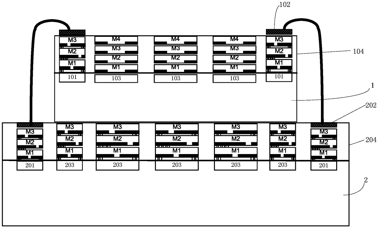
[0035] The present invention adopts an image sensor with an upper silicon chip and a lower silicon chip stacked, and the upper silicon chip and the lower silicon chip are connected by bonding wires; the upper silicon chip has a photosensitive sensor pixel array, and the readout circuit and output interface of the entire image sensor They are all arranged in the lower silicon chip, so that the integration degree of the lower silicon chip is undoubtedly increased. The present invention rationally constructs the highly integrated readout circuit and the interconnection...


PUM


Abstract

The invention provides a stacked image sensor, which is composed of an upper silicon chip and a lower silicon chip through stacking technology, wherein the upper silicon chip is a photosensitive sensor array, the lower silicon chip is a readout circuit and an output interface, and the upper and lower silicon chips are connected by binding line connected. The lower silicon wafer of the stacked image sensor is a readout circuit and an output interface. The readout circuit and output interface circuit of the entire stacked image sensor, including digital-to-analog converters, analog-to-digital converters, amplifiers, row and column controllers, digital algorithms, high-speed data interfaces, bandgap references, etc., are all contained in the lower silicon chip. By adopting a stacked image sensor, the high readout circuit and high-speed output circuit are transferred to the lower silicon chip of the stacked sensor, thereby effectively reducing the area of ​​the non-pixel array area in the upper silicon chip. The photosensitive fill rate of a single silicon chip can be improved by stacking the image sensor, which realizes low noise and low power consumption of the sensor chip, and greatly improves the fill factor of the photosensitive sensor pixel array.

Description

technical field [0001] The invention relates to the technical field of semiconductors, in particular to a stacked image sensor. Background technique [0002] Image sensors are an important part of digital cameras. According to the different components, it can be divided into two categories: CCD (Charge Coupled Device, charge-coupled device) and CMOS (Complementary Metal-Oxide Semiconductor, metal oxide semiconductor device). A prerequisite for the wide application of CMOS sensors is their higher sensitivity, shorter exposure time and shrinking pixel size. [0003] The front side illumination (FSI, Front Side Illumination) technology adopted by the traditional CMOS image sensor is the front illumination technology. The main feature of front-illumination technology is to fabricate photosensitive diodes, metal interconnections, and light pipe holes (Light Pipe) in sequence on the front of the silicon wafer. Its advantages are: simple process, fully compatible with CMOS proces...

Claims


Application Information

Patent Timeline
Patent Type & Authority Patents(China)
IPC IPC(8): H01L25/065H01L27/146
CPCH01L25/0657H01L27/14634H01L2225/06503H01L2224/48091H01L2224/48145H01L2924/00014
Inventor 李琛任铮雷冬梅张远皮常明温建新
Owner SHANGHAI INTEGRATED CIRCUIT RES & DEV CENT
Features
  • R&D
  • Intellectual Property
  • Life Sciences
  • Materials
  • Tech Scout
  • Unparalleled Data Quality
  • Higher Quality Content
  • 60% Fewer Hallucinations
Learn More