Manufacturing method of bonded structure and anisotropic conductive adhesive film

A connection structure, anisotropic technology, applied in the direction of conductive adhesive, film/sheet without carrier, connection, etc., can solve the problems of wiring hardening, difficult to obtain on-resistance, etc., and achieve the effect of excellent on-resistance

Active Publication Date: 2020-09-22
DEXERIALS CORP
View PDF1 Cites 0 Cited by
  • Summary
  • Abstract
  • Description
  • Claims
  • Application Information

AI Technical Summary

Problems solved by technology

[0003] However, conventional ultraviolet irradiation is mainly performed from the lower part of the substrate, so it is difficult to harden the wiring part with significantly low light transmittance, and it is difficult to obtain excellent on-resistance

Method used


Image

  • Manufacturing method of bonded structure and anisotropic conductive adhesive film
  • Manufacturing method of bonded structure and anisotropic conductive adhesive film
  • Manufacturing method of bonded structure and anisotropic conductive adhesive film

Examples


Embodiment

[0055]

[0056] Hereinafter, examples of the present invention will be described. In this example, an anisotropic conductive film was produced, bonded structures were fabricated using it at various irradiation timings, and the conduction resistance and curing rate of the bonded structures were evaluated. In addition, this invention is not limited to these Examples.

[0057] Production of the bonded structure, measurement of conduction resistance, and measurement and evaluation of the curing rate were performed as follows.

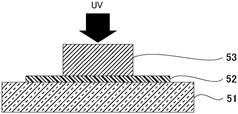
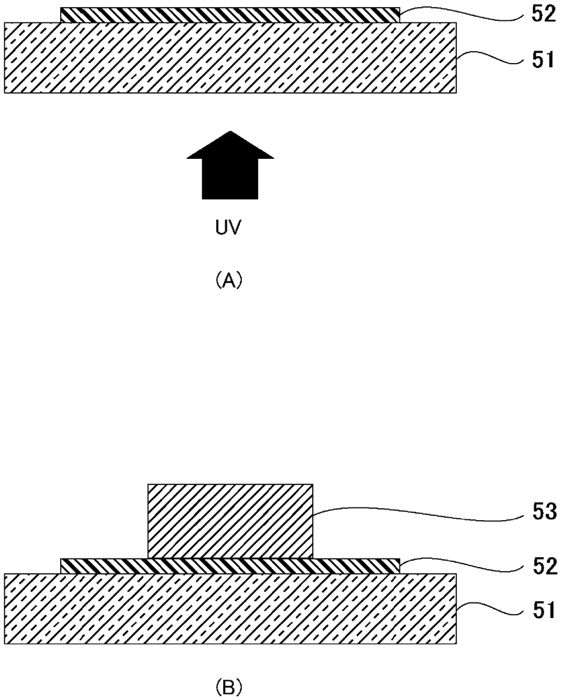
[0058] [Creation of connection structure]

[0059] As evaluation base materials, TI / Al plated glass substrates (metal wiring, t=0.7mm) and ICs (1.8mm×20mm, t=0.5mm, Au-plated bumps: 30μm×85μm, h=15μm) were used. The light irradiation condition is set to 200mW / cm 2 -3 seconds. In addition, the thermocompression bonding conditions were set at 120°C - 60 MPa - 5 seconds.

[0060] [Measurement of conduction resistance]

[0061] The conduction resistance...


PUM

PropertyMeasurementUnit
electrical resistanceaaaaaaaaaa

Abstract

The invention provides a method for manufacturing a connection structure and an anisotropic conductive adhesive film. The method comprises the following steps: light irradiation: irradiating UV rays on an anisotropic conductive film (20), wherein polymeric compounds and photopolymerization are in different parts of the anisotropic conductive film (20); hot pressure welding: subjecting first circuit part and second circuit part to hot pressure welding under the protection of the anisotropic conductive film (20). Because the hot pressure welding is carried out under the state that the photopolymerization initiator in the anisotropic conductive film is activated, the parts on which circuit is distributed can be fully cured, and thus excellent turn-on resistance can be obtained. Moreover, because the polymeric compounds and photopolymerization initiator are in different parts of the anisotropic conductive film, the hardening reactions are inhibited when the anisotropic conductive film is irradiated by UV rays, and the insufficient pressing due to early hardening is avoided.

Description

technical field [0001] This invention relates to the manufacturing method of the connection structure which electrically connects circuit components, and the anisotropic conductive film used for this method. Background technique [0002] Conventionally, in the connection of ACF (ACF: Anisotropic Conductive Film, anisotropic conductive film) such as LCD (Liquid Crystal Display, liquid crystal display) panels, the anisotropic conductive film is irradiated with ultraviolet light at a low temperature to make the anisotropic conductive film harden by reaction and lower the LCD panel. The warpage of the display can be suppressed (for example, refer to Patent Document 1.). [0003] However, conventional ultraviolet irradiation is mainly performed from the lower part of the substrate, so it is difficult to harden the wiring part with a remarkably low light transmittance, and it is difficult to obtain excellent on-resistance. [0004] Patent Document 1: Japanese Unexamined Patent Pu...

Claims


Application Information

Patent Timeline
Patent Type & Authority Patents(China)
IPC IPC(8): H01R43/00H01R4/04C09J7/10C09J9/02C09J163/00C09J171/12
Inventor 平山坚一
Owner DEXERIALS CORP
Why Eureka
Try Eureka