an etching method

A technology of lithography and trenching, which is applied in the direction of semiconductor devices, electrical components, circuits, etc., can solve the problems of inability to form contact holes, difficulty in lithography and etching of contact holes, etc., and solve the problem of difficulty in lithography and etching. Large, well-filled, reduced-impact effects

Active Publication Date: 2018-06-05
FOUNDER MICROELECTRONICS INT
View PDF3 Cites 0 Cited by
  • Summary
  • Abstract
  • Description
  • Claims
  • Application Information

AI Technical Summary

Problems solved by technology

[0004] Since the trench VDMOS is designed differently for different devices, the distance between the trenches is large or small. When the distance between the trenches is small, the polysilicon gate protrusion is high, resulting in the dielectric layer deposition in the subsequent process. The layers are connected or hollow, such as figure 1 and as figure 2 As shown, therefore, the prior art solution has the technical problem that the photolithography and etching of the contact hole are difficult when the dielectric layer is connected, and there is even a technical problem that the contact hole cannot be formed when the dielectric layer is hollow.

Method used


Image

  • an etching method
  • an etching method
  • an etching method

Examples


Embodiment Construction

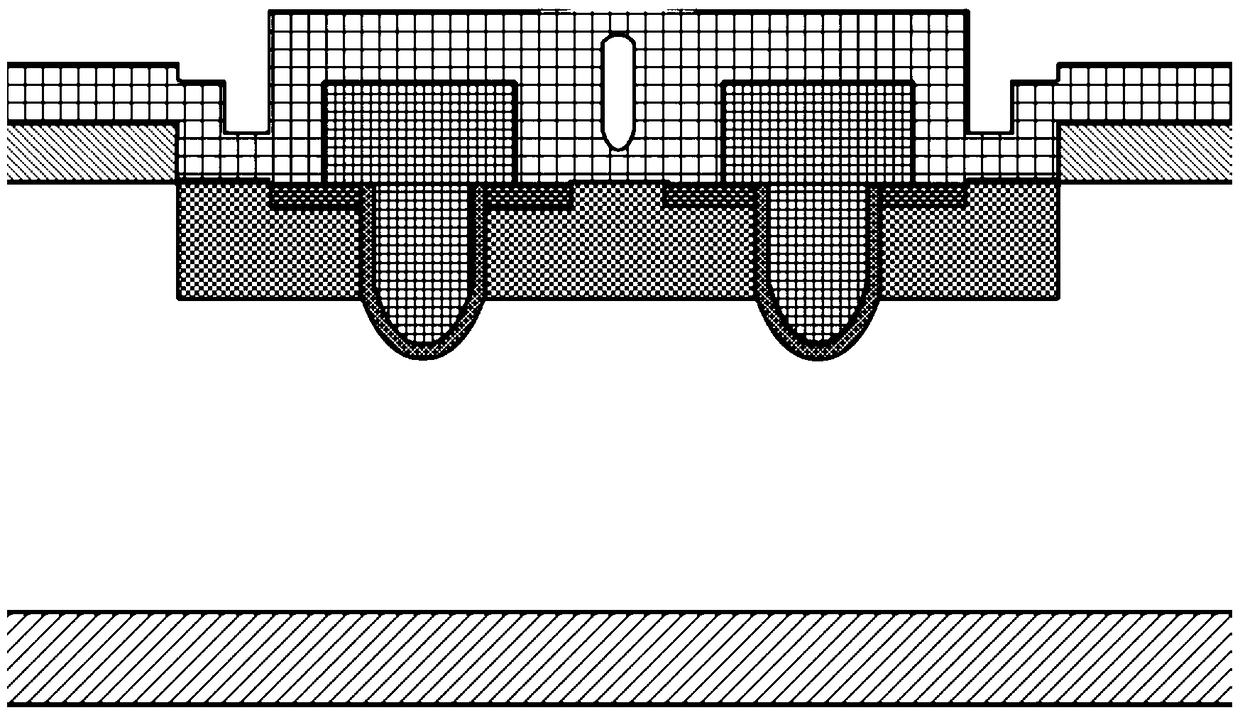
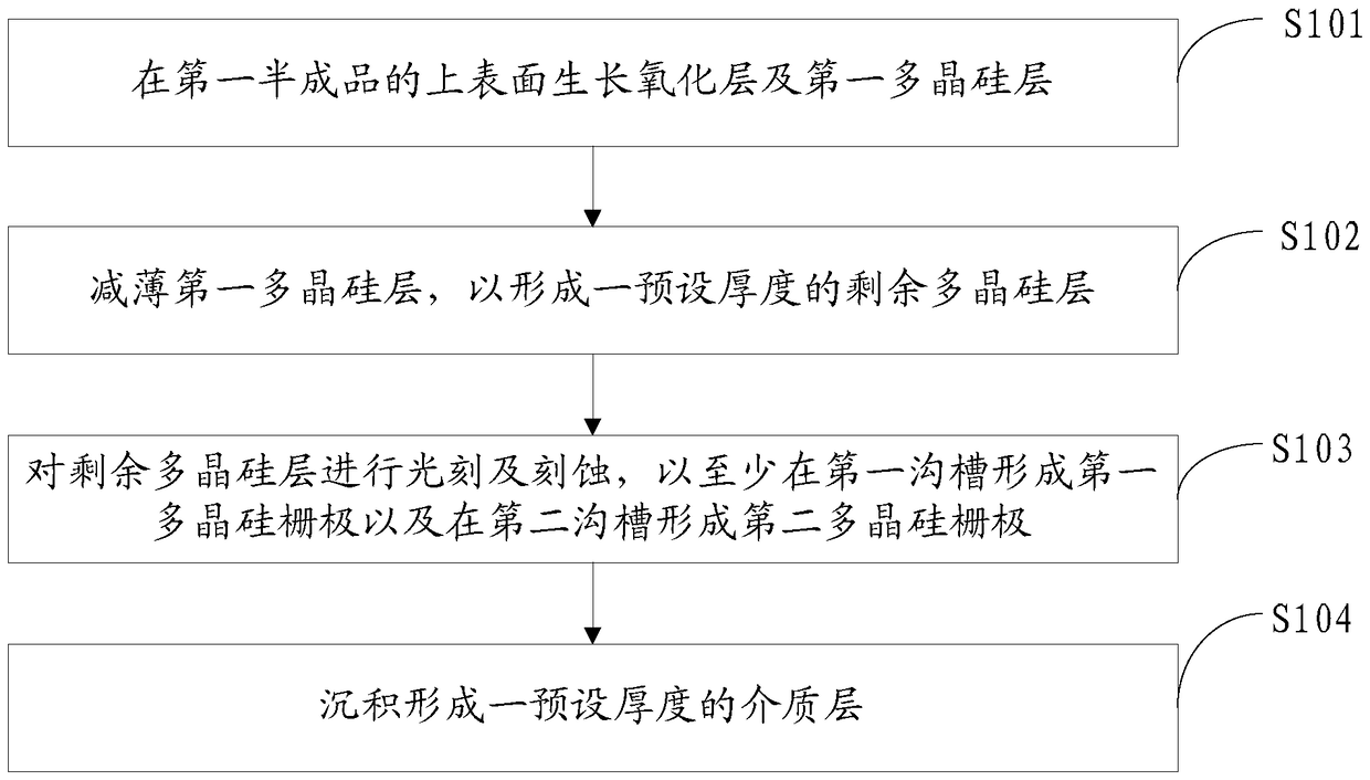
[0027] An embodiment of the present invention provides an etching method for processing a first semi-finished product used to manufacture a trench VDMOS device, the first semi-finished product includes a first substrate, and forming an epitaxial layer, in which at least a first body region is formed, in which at least a first source region and a second source region adjacent to the first source region are formed, And a first trench formed by etching down in the first source region and a second trench formed by etching down in the second source region.

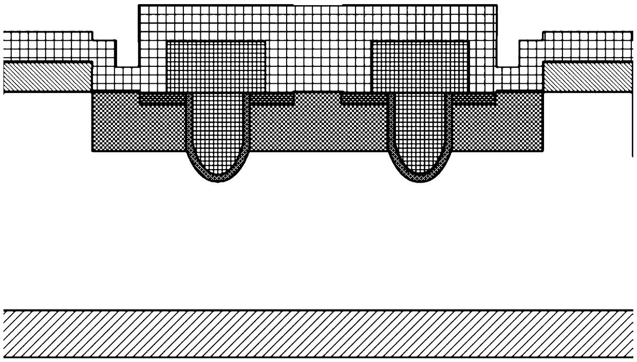
[0028] In the technical solution in the embodiment of the present invention, after growing the gate oxide layer and the first multi-silicon layer, etch the first polysilicon layer to a predetermined thickness of the remaining polysilicon layer, and then perform photolithography and etching on the remaining polysilicon layer eclipse. Because the growth thickness of polysilicon is related to the trench size, therefore, for VDMOS...


PUM


Abstract

The invention discloses an etching method, comprising: processing a first semi-finished product used to manufacture a trench VDMOS device, the first semi-finished product includes a first substrate, and forming an epitaxial layer, in which at least a first body region is formed, in which at least a first source region and a second source region adjacent to the first source region are formed, As well as a first trench formed by etching down in the first source region and a second trench formed by etching down in the second source region, the method includes: in the first semi-finished product growing a gate oxide layer and a first polysilicon layer on the upper surface; thinning the first polysilicon layer to form a remaining polysilicon layer with a predetermined thickness; performing photolithography and etching on the remaining polysilicon layer, A first polysilicon gate is formed at least in the first trench and a second polysilicon gate is formed in the second trench.

Description

technical field [0001] The invention relates to the field of semiconductor manufacturing, in particular to an etching method. Background technique [0002] VDMOS, that is, vertical double diffused metal-oxide semiconductor field effect transistor, VDMOS has the advantages of both bipolar transistors and ordinary MOS devices. Whether it is a switch application or a linear application, VDMOS is an ideal power device. VDMOS is mainly used in motor regulation. speed, inverter, uninterruptible power supply, electronic switch, hi-fi, automotive electrical appliances and electronic ballast, etc. Trench-type VDMOS adopts the trench etching technology invented in the preparation process of memory storage capacitors, so that the conductive trench changes from horizontal to vertical. Compared with the ordinary VDMOS structure, the resistance of the JFET neck area is eliminated. Therefore, the cell size is greatly increased. density, increasing the current handling capability of power ...

Claims


Application Information

Patent Timeline
Patent Type & Authority Patents(China)
IPC IPC(8): H01L21/336H01L21/28
Inventor 赵圣哲
Owner FOUNDER MICROELECTRONICS INT
Why Eureka
Try Eureka