LED (Light Emitting Diode) epitaxial wafer and preparation method therefor

An LED epitaxial wafer, low-temperature technology, applied in electrical components, circuits, semiconductor devices, etc., can solve problems such as segregation, and achieve the effect of reducing the degree of separation, improving the internal quantum efficiency, and reducing the phenomenon of segregation

Active Publication Date: 2016-03-23
XIANGNENG HUALEI OPTOELECTRONICS
View PDF3 Cites 5 Cited by
  • Summary
  • Abstract
  • Description
  • Claims
  • Application Information

AI Technical Summary

Problems solved by technology

[0004] The invention provides an LED epitaxial wafer and a preparation method thereof to solve t

Method used


Image

  • LED (Light Emitting Diode) epitaxial wafer and preparation method therefor
  • LED (Light Emitting Diode) epitaxial wafer and preparation method therefor
  • LED (Light Emitting Diode) epitaxial wafer and preparation method therefor

Examples


preparation example Construction

[0050] Another aspect of the present invention provides a method for preparing the above-mentioned LED epitaxial wafer, comprising the following steps:

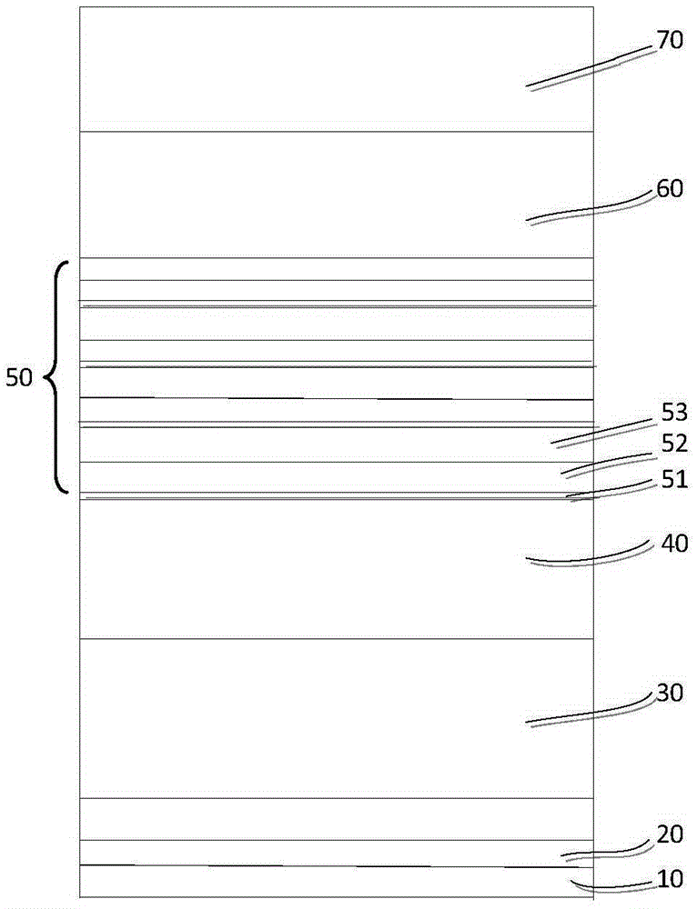
[0051] A low-temperature buffer GaN layer 20 , an undoped GaN layer 30 and an N-type GaN layer 40 are grown sequentially on the substrate 10 .

[0052] A multi-period quantum well layer 50 is set on the undoped GaN layer 30, and in any period, the x Ga 1-x Before the N layer 52 and the GaN layer 53, the InN thin layer 51 is plated under the conditions of a coating time of 10-60 seconds, an indium source flow rate of 200-1500 sccm, a temperature of 700-750° C., and a pressure of 100-800 mbar.

[0053] A P-type AlGaN layer 60 and a P-type GaN layer 70 are sequentially plated.

[0054] AixtronMOCVD was used to grow LED epitaxial wafers. Low temperature buffer GaN layer 20, undoped GaN layer 30 and N-type GaN layer 40, In x Ga 1-x The N layer 52, the GaN layer 53, the plated P-type AlGaN layer 60, and the P-type GaN layer 70...

Embodiment 2

[0082] 1. Treat the sapphire substrate at high temperature for 3-5 minutes in a hydrogen atmosphere at 1000-1200°C.

[0083] 2. Lower the temperature to 530-560° C., and grow a low-temperature buffer GaN layer with a thickness of 20-30 nm on the sapphire substrate.

[0084] 3. Raise the temperature to 1000-1100°C and continue to grow 3-4um undoped GaN.

[0085] 4. Then firstly grow 3-4μm N-type GaN continuously doped with Si, and the Si doping concentration is 5E+18-2E+19.

[0086] 5. Periodically grow the light-emitting layer MQW, and grow In-doped 2.5-3nmIn at a low temperature of 700-750°C x Ga 1-x N, x=0.20-0.22 layers, and a 10-12nm GaN layer is grown at a high temperature of 800-850°C. In x Ga 1-x The number of N layer / GaN layer periods is 12. In each period of the quantum well In x Ga 1-x Before N grows, a certain flow rate of TMIn is introduced to prepare a thin layer of InN.

[0087] Preparation conditions of InN thin layer: coating time is 15 seconds, trimethy...

Embodiment 3

[0094] The difference between embodiment 3 and embodiment 2 is that the deposition time of the thin InN layer 51 is 30 seconds.


PUM

PropertyMeasurementUnit
Thicknessaaaaaaaaaa
Thicknessaaaaaaaaaa
Thicknessaaaaaaaaaa

Abstract

The present invention discloses an LED (Light Emitting Diode) epitaxial wafer and a preparation method therefor. The LED epitaxial wafer comprises a substrate, a low-temperature buffer GGaN layer, an undoped GaN layer, an N-type GaN layer, a multi-cycle quantum well layer, a P-type AlGaN layer and a P-type GaN layer, which are arranged sequentially from bottom to top. The multi-cycle quantum well layer comprises an InxGa1-xN layer/GaN layer from 6-14 cycles, and in any one cycle, the GaN layer is arranged on the In<x>Ga<1-x>N layer, and an InN thin layer is arranged below the In<x>Ga<1-x>N layer, and the thickness of the InN thin layer is 0.2-1nm, and x is 0.20-0.22. The InN thin layer enables In atoms to achieve a dynamic saturation balance before reaching the In<x>Ga<1-x>N layer, so that a segregation phenomenon of In in the In<x>Ga<1-x>N layer is reduced, thereby reducing a separation degree of electrons and a cavitation wave function caused by a quanta stark effect, so as to improve internal quanta efficiency of an LED.

Description

technical field [0001] The invention relates to the field of LEDs, in particular to an LED epitaxial wafer. In addition, the present invention also relates to a method for preparing the above-mentioned LED epitaxial wafer. Background technique [0002] In the LED market, the driving voltage of LED chips is now required to be low, especially under high current, the smaller the driving voltage, the better, and the higher the light efficiency, the better; the LED market value is reflected in (light effect) / unit price, the better the light effect, the higher the price High, so LED high light efficiency has always been the goal pursued by LED manufacturers and LED research institutes in colleges and universities. [0003] The light efficiency of LED is largely related to the material properties of the light-emitting layer, so making an excellent light-emitting layer is the key to improving the light efficiency of LEDs. The quantum wells of existing LED epitaxial wafers include ...

Claims


Application Information

Patent Timeline
IPC IPC(8): H01L33/06H01L33/32H01L33/00
CPCH01L33/0066H01L33/0075H01L33/06H01L33/325
Inventor 林传强苗振林卢国军
Owner XIANGNENG HUALEI OPTOELECTRONICS
Why Eureka
Try Eureka