External cavity narrow linewidth laser device

A laser and narrow linewidth technology, which is applied in the direction of lasers, laser components, semiconductor lasers, etc., can solve the problem that the coherent reception of high-order modulation formats cannot be met, the application prospects of optical transmitters and receivers are not large, and the increase in process and System complexity and other issues, to achieve the effect of reducing coupling coefficient and line width, reducing sensitivity, reducing cavity surface reflection

Active Publication Date: 2016-03-23
山东中科际联光电集成技术研究院有限公司
View PDF4 Cites 7 Cited by
  • Summary
  • Abstract
  • Description
  • Claims
  • Application Information

AI Technical Summary

Problems solved by technology

The linewidth of the laser will affect the phase noise characteristics of the signal, and the frequency instability will cause the frequency drift of the signal, both of which have an important impact on the sensitivity of the receiver
The 400Gbps coherent communication system generally requires the linewidth of the laser to be below 100kHz, while the linewidth of the 1.55μm and 1.3μm band distributed feedback semiconductor lasers routinely deployed in the current optical fiber communication system is generally on the order of 1-10MHz, which cannot meet high Requirements for coherent reception of modulation formats
However, due to limitations in size, structure and mass production, the application prospects in optical transmitters and receivers are not great.
For distributed feedback semiconductor lasers or Bragg mirror lasers, by optimizing the device structure and some external linewidth compression methods, the linewidth can be controlled at the order of kilohertz, but at the same time, the complexity of the process and system is also increased, making it difficult mass production and application

Method used


Image

  • External cavity narrow linewidth laser device
  • External cavity narrow linewidth laser device
  • External cavity narrow linewidth laser device

Examples


Embodiment Construction

[0048] In order to make the object, technical solution and advantages of the present invention clearer, the present invention will be described in further detail below in conjunction with specific embodiments and with reference to the accompanying drawings.

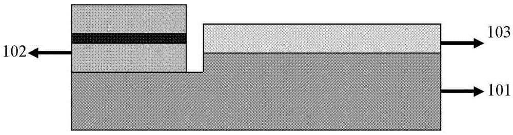
[0049] Figure 1a is a schematic cross-sectional view of an external cavity narrow linewidth laser according to an embodiment of the present invention, such as Figure 1a As shown, the external cavity narrow linewidth laser includes: a semiconductor optical amplifier 102, a planar waveguide grating 103 and a substrate 101, wherein:

[0050] The semiconductor optical amplifier 102 and the planar waveguide grating 103 are bonded to the substrate 101 by bonding to reduce the sensitivity of the laser to vibration, increase the stability of the laser, and reduce the noise of the laser;

[0051] One end of the semiconductor optical amplifier 102 is coated with a high reflection film, and the other end is coated with a high trans...


PUM


Abstract

The invention discloses an external cavity narrow linewidth laser device. The laser device comprises a semiconductor light amplifier, a planar waveguide grating and a substrate. The semiconductor light amplifier and the planar waveguide grating are arranged on the substrate in a bonding way. A high-reflection film is plated on one end of the semiconductor light amplifier, and a high-transmittance film is plated on the other end. The high-transmittance film is plated on the two sides of the planar waveguide grating respectively. The end surface of one end of the semiconductor light amplifier with plating of the high-transmittance film is coupled with the end surface of one side of the planar waveguide grating. The external cavity narrow linewidth laser device has the characteristics of narrow linewidth, high power, low noise and high frequency stability and can be applied to a high-order modulation format and a coherent detection system so as to provide a transmitting source and an intrinsic source laser device for the next generation of optical fiber communication system.

Description

technical field [0001] The invention relates to the technical field of semiconductor lasers, in particular to an external cavity narrow linewidth laser. Background technique [0002] With the rapid development of Internet communication, people's demand for communication capacity has increased sharply, and the single-channel communication capacity has begun to move towards 400Gbps. In order to increase the communication rate and spectral efficiency, new modulation formats and coherent detection systems are required. Higher-order modulation formats impose more stringent requirements on the linewidth and frequency stability of the emitter and local oscillator lasers. The linewidth of the laser will affect the phase noise characteristics of the signal, and the frequency instability will cause the frequency drift of the signal, both of which have an important impact on the sensitivity of the receiver. The 400Gbps coherent communication system generally requires the linewidth of...

Claims


Application Information

Patent Timeline
Patent Type & Authority Applications(China)
IPC IPC(8): H01S5/14H01S5/06H01S5/343
CPCH01S5/06H01S5/141H01S5/34306
Inventor 刘建国于丽娟苏亚嫚祝宁华
Owner 山东中科际联光电集成技术研究院有限公司
Why Eureka
Try Eureka