
Method for making silicon micro-nano structure array based on ultrasonic standing wave field

A technology of ultrasonic standing wave and standing wave field, which is applied in the manufacture of microstructure devices, microstructure technology, microstructure devices, etc., and can solve problems such as low cost performance and complicated operation of preparing regular micro-nano structures

Inactive Publication Date: 2016-03-30
HANGZHOU DIANZI UNIV
View PDF5 Cites 11 Cited by
  • Summary
  • Abstract
  • Description
  • Claims
  • Application Information

AI Technical Summary

Problems solved by technology

However, the metal-assisted chemical etching method is random, and the preparation of regular micro-nano structures is complicated and cost-effective.

Method used


Image

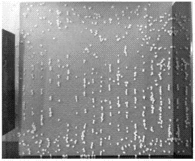
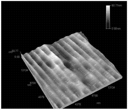
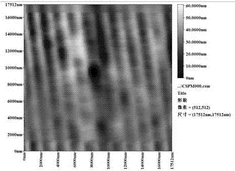
  • Method for making silicon micro-nano structure array based on ultrasonic standing wave field
  • Method for making silicon micro-nano structure array based on ultrasonic standing wave field
  • Method for making silicon micro-nano structure array based on ultrasonic standing wave field

Examples


Embodiment 1

[0033] Place the plastic reactor in the ultrasonic standing wave field formed by the ultrasonic generator, and the corrosion solution consists of HF solution, H 2 o 2 solution and AgNO 3 The composition of the solution is 5:2:3 by volume. Turn on the ultrasonic power supply, put the clean single crystal silicon silicon wafer into the reaction kettle, take it out after 30-60 minutes of etching time at room temperature, wash and dry it, and obtain the silicon micro-nano structure array.

Embodiment 2

[0035] Place the reaction kettle made of corrosive liquid in the ultrasonic standing wave field, and the corrosive liquid is composed of HF solution and H 2 o 2 The composition of the solution is 5:2 by volume. Turn on the ultrasonic power supply, put the silicon chip plated with silver by magnetron sputtering into the reaction kettle, take it out after 30-60 minutes of etching time at room temperature, wash and dry it, and obtain the silicon micro-nano structure array.

Embodiment 3

[0037] Place the reaction kettle made of corrosive liquid in the ultrasonic standing wave field, and the corrosive liquid is composed of HF solution and H 2 o 2 The composition of the solution is 5:2 by volume. Turn on the ultrasonic power supply, put the chemically silver-plated silicon chip into the reaction kettle, take it out after 30-60 minutes of etching time at room temperature, wash and dry it, and obtain the silicon micro-nano structure array.

[0038] The method of the present invention is based on the ultrasonic standing wave field to prepare the silicon micro-nano structure array, which combines the traditional metal-assisted chemical etching method with the ultrasonic standing wave field. In the ultrasonic standing wave field, the metal catalyst particles in the metal-assisted chemical etching Under the action of the acoustic radiation force, it accumulates at the standing wave point to form a local directional corrosion to prepare a regular array of micro-nano s...


PUM


Abstract

The invention discloses a method for making a silicon micro-nano structure array based on an ultrasonic standing wave field. The method comprises the following steps: (1) preparing corrosive liquid, wherein the corrosive liquid is prepared from an HF solution, an H<2>O<2> solution and an AgNO<3> solution which are mixed uniformly; (2) putting the corrosive liquid obtained in the step (1) into a reaction kettle, putting the reaction kettle into the ultrasonic standing wave field formed by an ultrasonic generator, and starting an ultrasonic power supply to form the ultrasonic standing wave field; and (3) putting cleaned monocrystalline silicon wafers into the reaction kettle, and corroding the monocrystalline silicon wafers for 30-60 minutes to obtain a monocrystalline silicon micro-nano structure array. Through adoption of the method, the ultrasonic standing wave field is combined with a conventional metal-assisted chemical corrosion method, so that metal catalyst particles are accumulated on ultrasonic standing wave points under the action of acoustic radiation force of the ultrasonic standing wave field in a reaction process; the metal catalyst particles are distributed on a monocrystalline silicon surface in a linear array form; and a regular micro-nano structure array is formed on the monocrystalline silicon surface along with the proceeding of a corrosive reaction.

Description

technical field [0001] The invention belongs to the technical field of micro-nano processing, and in particular relates to a method for preparing a silicon micro-nano structure array based on an ultrasonic standing wave field. Background technique [0002] As an important semiconductor material, silicon is widely used in sensors, solar cells, MEMS and other fields, and plays a very important role. At present, the methods for preparing micro-nano structures on single crystal silicon mainly include vapor-liquid-solid (VLS) method, reactive ion etching method, spot chemical etching method and metal-assisted chemical etching method. Among them, the metal-assisted chemical etching method is cost-effective, the processing method is simple and easy, the preparation of micro-nano structures is easy to control, and the processing quality is high. Therefore, it is widely used at present. However, the metal-assisted chemical etching method is random, and the preparation of regular mi...

Claims


Application Information

Patent Timeline
Patent Type & Authority Applications(China)
IPC IPC(8): B81C1/00B82Y40/00H01L31/0236
CPCY02E10/50B81C1/00539B82Y40/00H01L31/02363
Inventor 巢炎姚安琦焦晓东吴立群刘先欢王盛
Owner HANGZHOU DIANZI UNIV
Learn More