Forming method of tungsten electrode

A technology of tungsten electrodes and tungsten layers, which is applied in the manufacture of circuits, electrical components, semiconductors/solid-state devices, etc., can solve the problems that the performance of tungsten electrodes cannot meet the development requirements of semiconductor devices, and achieve the effect of improving performance and increasing the formation rate

Inactive Publication Date: 2016-03-30
SEMICON MFG INT (SHANGHAI) CORP
View PDF16 Cites 4 Cited by
  • Summary
  • Abstract
  • Description
  • Claims
  • Application Information

AI Technical Summary

Problems solved by technology

But in practice, refer to Figure 4 , because the aspect ratio of the opening 19 is still relatively large, when the opening 19 is filled with tungsten 142, a void

Method used


Image

  • Forming method of tungsten electrode
  • Forming method of tungsten electrode
  • Forming method of tungsten electrode

Examples


Embodiment Construction

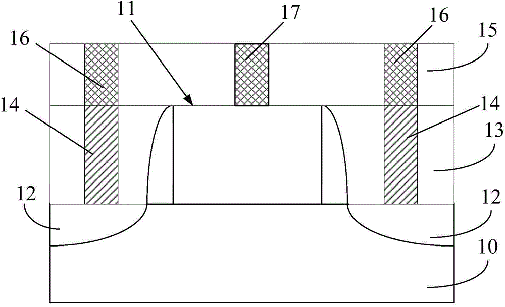
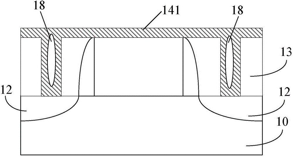
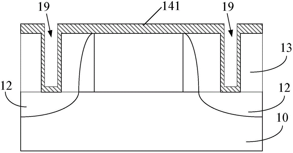
[0046] As mentioned in the background technology, with the development of semiconductor devices, the precision requirements of corresponding semiconductor devices are continuously improved. However, when forming a semiconductor device with a multi-layer structure in the existing process, it is placed in the dielectric layer and used to connect transistors and other layers. Voids will form in the tungsten electrode of the semiconductor element, thereby reducing the performance of the tungsten electrode, thereby affecting the performance of the semiconductor device. Especially with the development of semiconductor devices, the aspect ratio of openings used to form tungsten electrodes is increasing, and the defects of voids in tungsten electrodes are more obvious, which has a greater impact on semiconductor devices with increasing precision requirements.

[0047]Analyzing the reason, with the development of semiconductor technology, the aspect ratio used to form the through hole o...


PUM


Abstract

The invention provides a forming method of a tungsten electrode. The method comprises the steps of: forming a first opening in a semiconductor substrate, forming a tungsten layer respectively on the side wall and the bottom part of the first opening and the surface of the semiconductor substrate, then removing the tungsten layer on the surface of the semiconductor substrate, and at least reserving a part of tungsten layer on the bottom part of the first opening; and then using the residual tungsten layer in the first opening as a core layer, and continuously forming tungsten to fill the first opening. After tungsten on the surface of the first opening is removed, tungsten cannot be formed on the surface of the semiconductor surface in the tungsten forming process with the residual tungsten layer in the first opening used as the core layer, so that the first opening is prevented from being blocked by tungsten on the surface of the semiconductor substrate, and the problem that reaction gas fails to enter the first opening is solved, the number and size of gaps in tungsten formed in the opening are further reduced, and the performance of the tungsten electrode is improved.

Description

technical field [0001] The invention relates to the field of semiconductor manufacturing, in particular to a method for forming a tungsten electrode. Background technique [0002] With the rapid development of integrated circuit (abbreviated as IC) manufacturing technology, the process nodes of traditional integrated circuits are gradually reduced, and the size of integrated circuit devices is continuously reduced. On a wafer, the number of semiconductor components is continuously increased. Processes are constantly being innovated to improve the performance of integrated circuit devices. [0003] For example, in order to meet the requirements of increasing the number of semiconductor elements, a wafer often includes semiconductor elements with a multi-layer structure, and the semiconductor elements of adjacent layers are electrically connected through a metal interconnection structure, thereby increasing the number of semiconductor elements on a chip with a specific area. ...

Claims


Application Information

Patent Timeline
IPC IPC(8): H01L21/28H01L21/768
Inventor 徐建华
Owner SEMICON MFG INT (SHANGHAI) CORP
Why Eureka
Try Eureka