Backside-illuminated sensor and manufacturing process thereof

A manufacturing process and sensor technology, which is applied in the field of semiconductor manufacturing process, can solve the problems of low blue light absorption efficiency and the influence of absorption efficiency, etc., and achieve the effect of improving quantum efficiency, improving performance, and simple manufacturing process

Active Publication Date: 2016-03-30
WUHAN XINXIN SEMICON MFG CO LTD
View PDF3 Cites 1 Cited by
  • Summary
  • Abstract
  • Description
  • Claims
  • Application Information

AI Technical Summary

Problems solved by technology

[0003] However, part of the quantum efficiency (Quantumefficiency) loss of the existing second-generation back-illuminated sensors comes from the back film technology, including the reflection and scattering of different dielectric films; and the blue light absorption efficiency is not high on the basis of the existing film technology.
It is necessary to use different dielectric films to offset the loss of light, but once other dielectric films (such as silicon nitride) are added, the absorption efficiency of red and green light will be affected accordingly

Method used


Image

  • Backside-illuminated sensor and manufacturing process thereof
  • Backside-illuminated sensor and manufacturing process thereof
  • Backside-illuminated sensor and manufacturing process thereof

Examples


Embodiment Construction

[0038] see figure 1 With the structure shown, the invention discloses a manufacturing process of a back-illuminated sensor, which specifically includes:

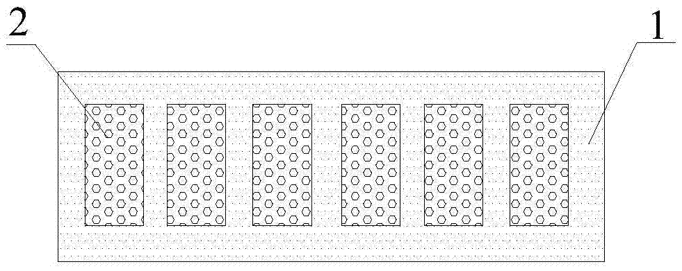
[0039] First, provide a silicon substrate 1 with a number of photodiodes 2 prepared inside, wherein the photodiodes 2 are prepared inside the silicon substrate 1, and each photodiode is provided with a photodiode adjacent to the photodiode. To prevent the two from contacting and conducting, at the same time, polysilicon in the silicon substrate is in contact with each surface of the photodiode to prevent the photodiode from contacting with other conductive devices or being exposed on the surface of the silicon substrate 1. The photodiode is damaged , see for details figure 2 The schematic diagram of the structure is shown.

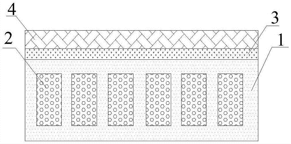
[0040] Continue to prepare a high-K dielectric material layer 3 and a buffer layer 4 sequentially on the silicon substrate to form a image 3 As shown in the schematic diagram of the structure, prefe...


PUM


Abstract

The invention relates to the technical field of semiconductor preparation processes, and especially relates to a backside-illuminated sensor manufacturing process. The manufacturing process comprises the following steps: providing a silicon substrate in which a plurality of photodiodes are prepared; sequentially preparing a high-K dielectric material layer, a buffer layer and a medium layer on the silicon substrate; etching the medium layer to the upper surface of the buffer layer to form a plurality of openings in the medium layer; and filling the openings with an oxide material layer to form a backside-illuminated sensor of which the medium layer is inlaid with the oxide material layer. The backside-illuminated sensor preparation process disclosed by the technical scheme is simple, can meet the requirements of different backside illumination processes, improves the quantum efficiency, and improves the performance of chips.

Description

technical field [0001] The invention relates to the technical field of semiconductor preparation technology, in particular to a back-illuminated sensor manufacturing technology. Background technique [0002] As a type of camera chip, back-illuminated image sensors have already occupied most of the market. The performance requirements of major manufacturers for back-illuminated image sensors are also getting higher and higher. The performance requirements are mainly reflected in: reducing dark current, Reduce noise, improve signal-to-noise ratio; increase quantum conversion rate, improve sharpness; higher pixels and resolution. [0003] However, part of the quantum efficiency (Quantumefficiency) loss of the existing second-generation back-illuminated sensors comes from the back-side thin-film technology, including the reflection and scattering of different dielectric films; and the blue light absorption efficiency is not high on the basis of the existing thin-film technology....

Claims


Application Information

Patent Timeline
Patent Type & Authority Applications(China)
IPC IPC(8): H01L27/146
CPCH01L27/14625H01L27/1464H01L27/14685
Inventor 胡胜
Owner WUHAN XINXIN SEMICON MFG CO LTD
Why Eureka
Try Eureka