Silicon through hole test circuit and method thereof, test circuit of silicon through hole group in three-dimensional integrated circuit and method thereof

A technology for testing circuits and through-silicon vias, which is applied in the direction of circuits, semiconductor/solid-state device testing/measurement, electrical components, etc. It can solve problems such as TSV open circuit, void, crack, and TSV resistance increase, and achieve the goal of improving yield Effect

Active Publication Date: 2016-04-06
PEKING UNIV SHENZHEN GRADUATE SCHOOL
View PDF5 Cites 9 Cited by
  • Summary
  • Abstract
  • Description
  • Claims
  • Application Information

AI Technical Summary

Problems solved by technology

figure 1 The open-circuit defects shown in (b) are mainly caused by voids and cracks in the TSV metal conductors. The main electrical manifestation of these defects is that the TSV resistance increases, and even leads to TSV open-circuit in severe cases.
figure 1 The main reason for the short-...

Method used


Image

  • Silicon through hole test circuit and method thereof, test circuit of silicon through hole group in three-dimensional integrated circuit and method thereof
  • Silicon through hole test circuit and method thereof, test circuit of silicon through hole group in three-dimensional integrated circuit and method thereof
  • Silicon through hole test circuit and method thereof, test circuit of silicon through hole group in three-dimensional integrated circuit and method thereof

Examples


Embodiment Construction

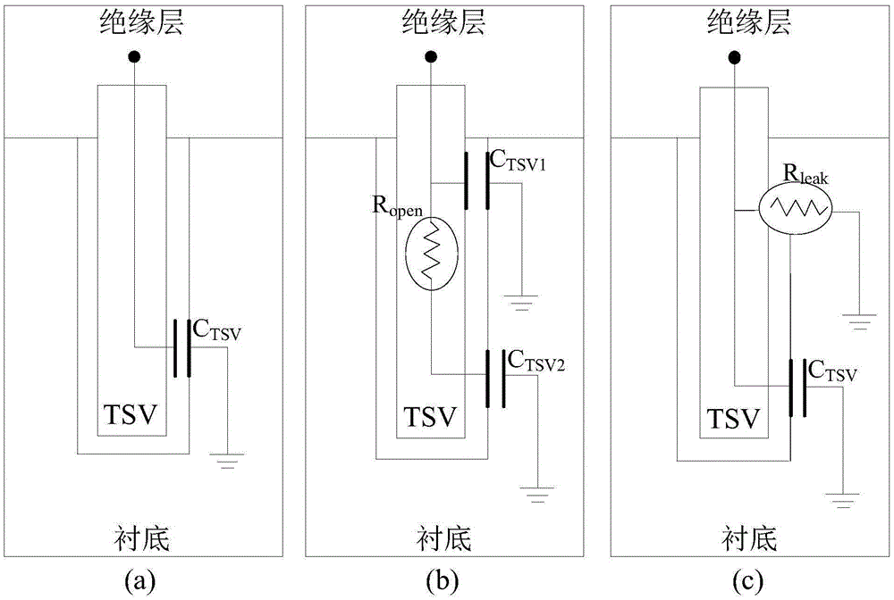
[0041] Due to the characteristics of the three-dimensional integrated circuit process, the TSV test needs to be divided into two stages: pre-bond and post-bond. In the pre-bond test stage, TSVs are usually in the form of blind holes, and TSVs can usually be contacted by test probes, and some testability design schemes can also be used to assist. In the post-bond stage, the interlayer stacking interconnection of chips has been completed, and TSVs have been buried in the stack to play the role of interlayer interconnection. At this point, probe contact of the TSV becomes very difficult or even impossible.

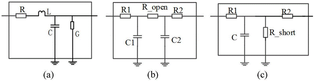
[0042] Such as figure 2 , where (a), (b), and (c) show schematic diagrams of the circuit model of TSV and its open and short defects, respectively.

[0043] Such as figure 2 As shown in (b), during the open defect test, a pulse signal is input to the TSV. Since the parasitic RC parameters in the TSV are very small, the rise and fall times of the signal passing through t...


PUM


Abstract

The invention relates to a silicon through hole test circuit and a method thereof, a test circuit of a silicon through hole group in a three-dimensional integrated circuit and a method thereof. The circuit comprises an excitation source, two parallel circuit branches, a third circuit branch and a detection circuit branch, wherein the excitation source is connected to an input terminal of a TSV and is used for providing an excitation signal; the two parallel circuit branches are connected to an output terminal of the TSV; one circuit branch comprises an inverting device and the other circuit branch comprises a level trigger device and a switch device; the switch device is used for controlling on and off of the circuit branch where the level trigger device is located; the third circuit branch is connected to output terminals of the two parallel circuit branches and is used for giving corresponding output according to a current conduction or disconnection state of the circuit branch; and the detection circuit branch is used for determining whether the TSV has an open circuit defect or a short circuit defect according to an output signal presentation of the third circuit branch. Through analyzing the signal presentations of two circuit branch output terminals, the TSV defect is determined. Through using one set of test circuit, open circuit defect and short circuit defect tests can be covered.

Description

technical field [0001] The present application relates to the technical field of integrated circuit testing, in particular to a testing method and testing circuit for through-silicon vias in three-dimensional integrated circuits. Background technique [0002] Through Silicon Via (TSV, ThroughSiliconVia) is a component that realizes the interconnection between layers of three-dimensional (3D) integrated circuits, such as figure 1 As shown in (a), TSV usually consists of a metal conductor and an insulating protective layer. TSV directly passes through the silicon material vertically, connects circuits on different layers, and greatly reduces the length of interlayer interconnection lines of three-dimensional integrated circuits, thereby effectively improving circuit performance. [0003] It is inevitable that some physical defects will be introduced during the TSV manufacturing process. The TSV defects that are generally concerned by the industry at present mainly include op...

Claims


Application Information

Patent Timeline
IPC IPC(8): H01L23/544H01L21/66
CPCH01L23/544H01L22/12H01L22/14
Inventor 崔小乐井兵强金玉丰
Owner PEKING UNIV SHENZHEN GRADUATE SCHOOL
Why Eureka
Try Eureka