

Infrared light-emitting diode with strain harmony multi-quantum well structure
A multi-quantum well structure and infrared light-emitting technology, applied in the field of infrared light-emitting diodes, can solve problems such as difficulty in making monochromatic multi-quantum well structures and the like
- Summary
- Abstract
- Description
- Claims
- Application Information
AI Technical Summary
Problems solved by technology
Method used
Image

Examples
Embodiment 1
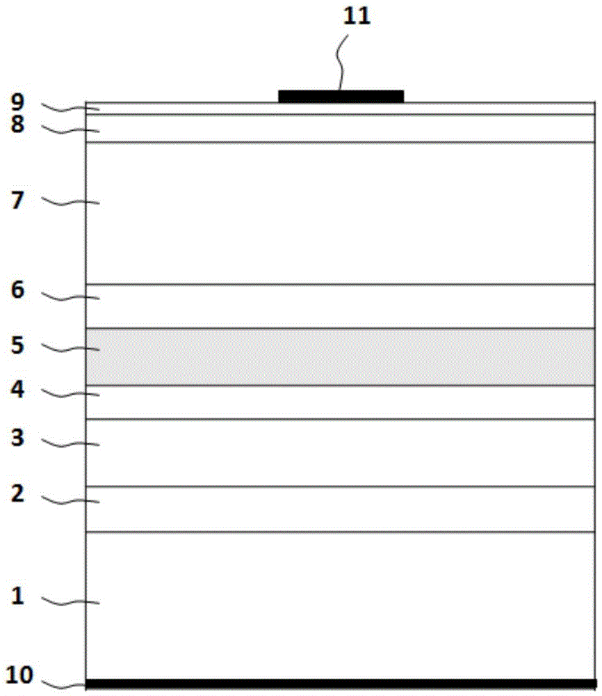
[0026] The contact layer is a P-type contact layer Al heavily doped with C X Ga 1-X As, where X is 35% and the concentration is 8E18 atoms / cm.
[0027] The P-type first cladding layer is a C-doped P-type first cladding layer Al X Ga 1-X As, wherein X is 15%, and the concentration is 8E17 atoms / cm; the P-type second cladding layer is a C-doped P-type second cladding layer Al X Ga 1-X As, where X is 35% and the concentration is 1E18 atoms / cm.
[0028] The N-type second cladding layer is an N-type second cladding layer Al doped with Si X Ga 1-X As, wherein X is 35%, and the concentration is 1E18 atoms / cm; the N-type first cladding layer is an N-type first cladding layer Al doped with Si X Ga 1-X As, where X is 15%, and the concentration is 6E17 atoms / cm.
[0029] The buffer layer is a buffer layer composed of GaAs, and the concentration is 1.5E18 atoms / cm.
[0030] The GaAs substrate is a single crystal N-type GaAs substrate doped with Si, and the concentration is 1.2E1...
Embodiment 2
[0035] The contact layer is a P-type contact layer Al heavily doped with C X Ga 1-X As, where X is 35% and the concentration is 8E18 atoms / cm.
[0036] The P-type first cladding layer is a C-doped P-type first cladding layer Al X Ga 1-X As, wherein X is 15%, and the concentration is 8E17 atoms / cm; the P-type second cladding layer is a C-doped P-type second cladding layer Al X Ga 1-X As, where X is 35% and the concentration is 1E18 atoms / cm.
[0037] The N-type second cladding layer is an N-type second cladding layer Al doped with Si X Ga 1-X As, wherein X is 35%, and the concentration is 1E18 atoms / cm; the N-type first cladding layer is an N-type first cladding layer Al doped with SiX Ga 1-X As, where X is 15%, and the concentration is 6E17 atoms / cm.
[0038] The buffer layer is a buffer layer composed of GaAs, and the concentration is 1.5E18 atoms / cm.
[0039] The GaAs substrate is a single crystal N-type GaAs substrate doped with Si, and the concentration is 1.2E18 ...
Embodiment 3
[0043] The contact layer is a P-type contact layer Al heavily doped with C X Ga 1-X As, where X is 35% and the concentration is 8E18 atoms / cm.
[0044] The P-type first cladding layer is a C-doped P-type first cladding layer Al X Ga 1-X As, wherein X is 15%, and the concentration is 8E17 atoms / cm; the P-type second cladding layer is a C-doped P-type second cladding layer Al X Ga 1-X As, where X is 35% and the concentration is 1E18 atoms / cm.
[0045] The N-type second cladding layer is an N-type second cladding layer Al doped with Si X Ga 1-X As, wherein X is 35%, and the concentration is 1E18 atoms / cm; the N-type first cladding layer is an N-type first cladding layer Al doped with Si X Ga 1-X As, where X is 15%, and the concentration is 6E17 atoms / cm.
[0046] The buffer layer is a buffer layer composed of GaAs, and the concentration is 1.5E18 atoms / cm.
[0047] The GaAs substrate is a single crystal N-type GaAs substrate doped with Si, and the concentration is 1.2E1...
PUM
| Property | Measurement | Unit |
|---|---|---|
| Thickness | aaaaa | aaaaa |
| Thickness | aaaaa | aaaaa |
| Thickness | aaaaa | aaaaa |
Abstract
Description
Claims
Application Information