Method for growing large-size and low-defect silicon carbide monocrystal and wafer

A silicon carbide single crystal, low-defect technology, applied in chemical instruments and methods, single crystal growth, crystal growth, etc., can solve problems such as dislocation defects in large-diameter SiC crystals

Inactive Publication Date: 2016-04-27
CHINA ELECTRONIC TECH GRP CORP NO 2 RES INST
View PDF8 Cites 7 Cited by
  • Summary
  • Abstract
  • Description
  • Claims
  • Application Information

AI Technical Summary

Problems solved by technology

[0003] The invention provides a method for growing large-size low-defect silicon carbide single c

Method used


Image

  • Method for growing large-size and low-defect silicon carbide monocrystal and wafer
  • Method for growing large-size and low-defect silicon carbide monocrystal and wafer
  • Method for growing large-size and low-defect silicon carbide monocrystal and wafer

Examples


Embodiment Construction

[0021] The present invention is described in detail below in conjunction with the accompanying drawings:

[0022] A method for growing large-scale low-defect silicon carbide single crystals and wafers, comprising the steps of:

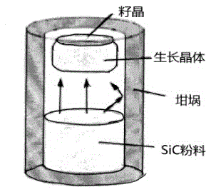
[0023] 1. Use the mainstream {0001} plane or {0001} plane off-angle direction 0, 4 degree SiC wafer as the seed crystal for growth, especially, there is no special requirement for its defects, and there are many defects and Less defects are available, (the level of SiC wafers purchased on the market is determined by the number of defects, the higher the level, the higher the price). In addition, the seed crystal diameter must be the desired wafer diameter plus 0.5 to 1 inch (due to the large radial temperature gradient at the crystal edge during growth and the interference of the lining edge, the quality of the crystal edge is poor, and high-quality crystals must be obtained And wafers need to remove the part with poor edge quality during processing,...


PUM


Abstract

The invention discloses a method for growing large-size and low-defect silicon carbide monocrystal and wafer, and is used for solving the problem of dislocation defects in a large-diameter SiC crystal. The method comprises the steps: adopting large-diameter SiC wafer having more or less defects and basically parallel to a (0001) plane as a seed crystal, and growing to obtain an SiC crystal ingot; processing the crystal ingot to obtain a wafer with largest deflection angle, and taking the wafer as a seed crystal; repeating the steps until a growing plane of the crystal ingot is substantially parallel to a (11-20) plane or a (1-100) plane; and after repeating the steps at the plane for multiple times, making the growing plane of the crystal ingot substantially parallel to the (0001) plane according to reverse steps, and processing to obtain an SiC wafer with a required deflection angle in the meanwhile. The continuity of growth of the SiC wafer with large diameter and low defect density is guaranteed.

Description

technical field [0001] The invention provides a method for preparing SiC single crystal with low defect density and processing SiC wafer. Background technique [0002] Silicon carbide (SiC) is a third-generation wide-bandgap semiconductor material with properties such as wide bandgap, high thermal conductivity, high electron saturation migration rate, and high breakdown electric field. Ideal semiconductor material for electronic devices. Commonly used SiC is mostly α phase (4H, 6H), which has a wide band gap and can be used in high-power electronic devices; SiC growth is mostly used for (0001) plane or (0001) plane biased <11-20> direction 0- According to the crystal growth theory, the (0001) plane growth of SiC single crystal belongs to the growth of screw dislocation mechanism, and the defects such as micropipes and dislocations on the growth surface provide the source of steps for crystal growth. Most of the defects in the crystal are inherited from the seed cryst...

Claims


Application Information

Patent Timeline
IPC IPC(8): C30B29/36C30B23/00
CPCC30B29/36C30B23/00
Inventor 戴鑫王英民李斌毛开礼王利忠马康夫徐伟周立平何超侯晓蕊田牧
Owner CHINA ELECTRONIC TECH GRP CORP NO 2 RES INST
Why Eureka
Try Eureka