

A method of electroplating silicon -based TSV rotor board
An adapter board, silicon-based technology, applied in the manufacturing of circuits, electrical components, semiconductor/solid-state devices, etc., can solve the problem of difficult and no-hole filling, and achieve the effect of good electrical conductivity, strong flexibility, and simplified process steps
- Summary
- Abstract
- Description
- Claims
- Application Information
AI Technical Summary
Problems solved by technology
Method used
Image

Examples
Embodiment 1
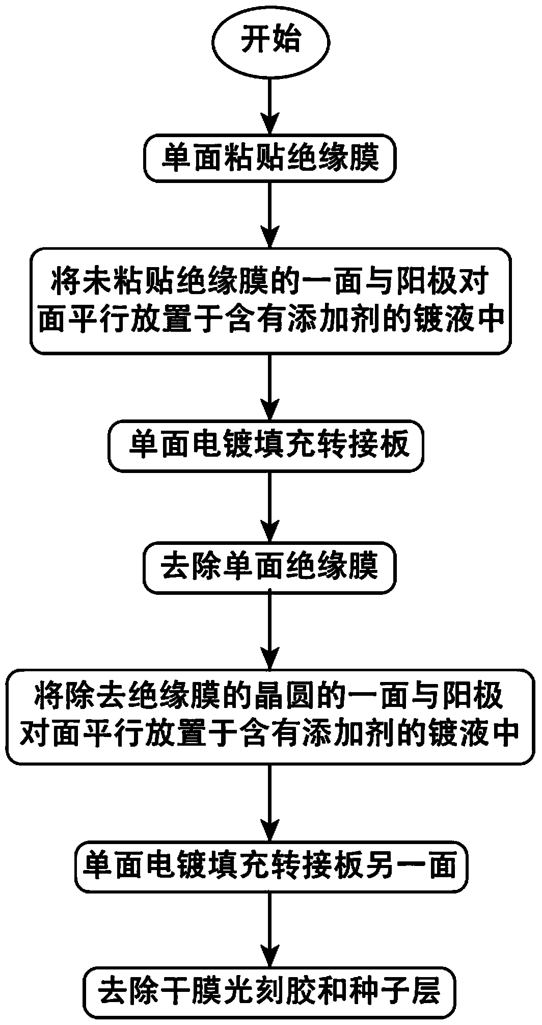
[0037] In this embodiment, an insulating film is pasted on one side of the TSV wafer by hot pressing or pasting technology, pre-wetting treatment is performed before primary electroplating, and the TSV and the Pad area are filled by electroplating technology. The wafer with the TSV through hole etched can be prepared in advance, and the silicon dioxide insulating layer, titanium barrier layer and copper seed layer can be prepared by thermal oxidation, sputtering and other methods.
[0038] The concrete steps of this embodiment:
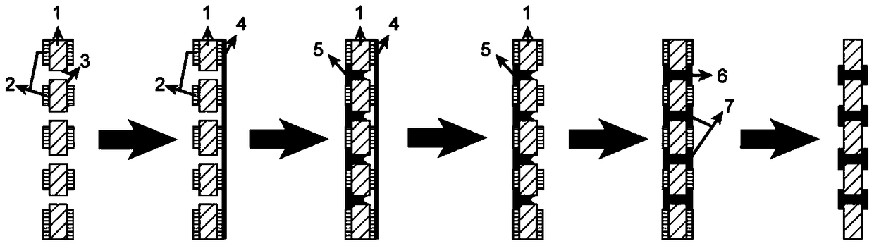
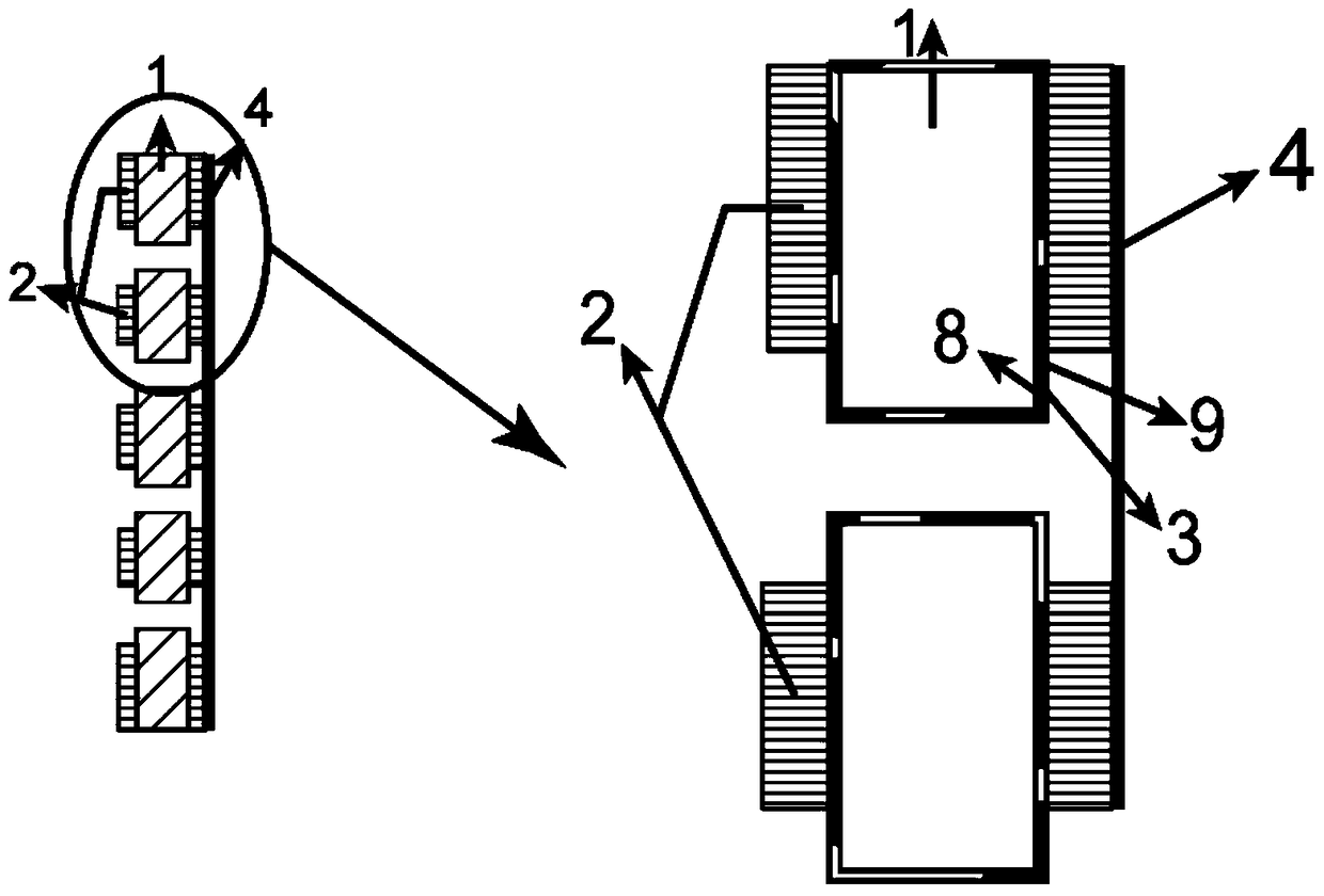
[0039] 1) Hot pressing or pasting an insulating film 4 on one side of a through-hole silicon wafer 1 with a double-sided dry film photoresist;
[0040] The through-hole silicon wafer 1 described in this embodiment can be prepared by the following method:
[0041] a. Spin-coat the silicon wafer with a positive glue of 10 μm or more or a negative glue of 10 μm or more, bake the glue with an oven or a hot plate, and perform photolithography and developm...
Embodiment 2
[0055] In this embodiment, the previous steps are the same as in Embodiment 1, except that there is no pre-wetting treatment before the first electroplating, but the pre-wetting step is placed before the second electroplating. An organic or inorganic insulating film is selected here.
[0056] 1) The well-prepared through-hole wafer with double-sided dry film photoresist is hot-pressed or pasted with an insulating film on one side;
[0057] 2) The wafer containing through holes with different apertures treated in step 1) is placed in a plating solution containing additives (accelerator SPS, inhibitor PEG and leveler JGB) in parallel with the anode on the side where the insulating film is not pasted. ;
[0058] 3) Using electroplating technology to fill the through-silicon vias TSV and Pad processed in step 2) on one side (one-time electroplating);
[0059] 4) After the Cu-Pad on the side not covered by the insulating film is formed by electroplating, remove the insulating fil...
PUM
 Abstract
Description
Claims
Application Information