Chemical palladium plating method for back through hole metallization seed layer of semiconductor

A semiconductor and electroless plating technology, applied in semiconductor devices, semiconductor/solid-state device manufacturing, electrical components, etc., can solve problems such as high process cost, uneven metal layer thickness, faults, etc., achieve broad market prospects, wide application range, Good quality workmanship

Inactive Publication Date: 2016-05-04
NO 55 INST CHINA ELECTRONIC SCI & TECHNOLOGYGROUP CO LTD
View PDF5 Cites 8 Cited by
  • Summary
  • Abstract
  • Description
  • Claims
  • Application Information

AI Technical Summary

Problems solved by technology

[0003] However, in practical applications, the coverage effect of sputtered metal is not ideal, especially in deep hole sputtering, the coverage of sputtered metal becomes worse with the increase of back hole depth; in addition, on the hole wall with more burrs, The thickness of the metal layer is very uneven, and the metal in the area blocked by the burr often has micro-breaks or even faults. In the subsequent electroplating process, these areas are prone to form bubbles or holes, and the electroplating effect is poor, which seriously affects the quality and reliability of the chip.
Moreover, the target utilization rate of the sputtering metal seed layer technology is low, and the process cost is high
The above defects limit the development of sputtering metal seed layer technology, making it difficult to be further promoted and applied

Method used


Image

  • Chemical palladium plating method for back through hole metallization seed layer of semiconductor
  • Chemical palladium plating method for back through hole metallization seed layer of semiconductor
  • Chemical palladium plating method for back through hole metallization seed layer of semiconductor

Examples


Embodiment Construction

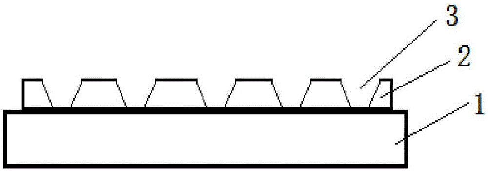
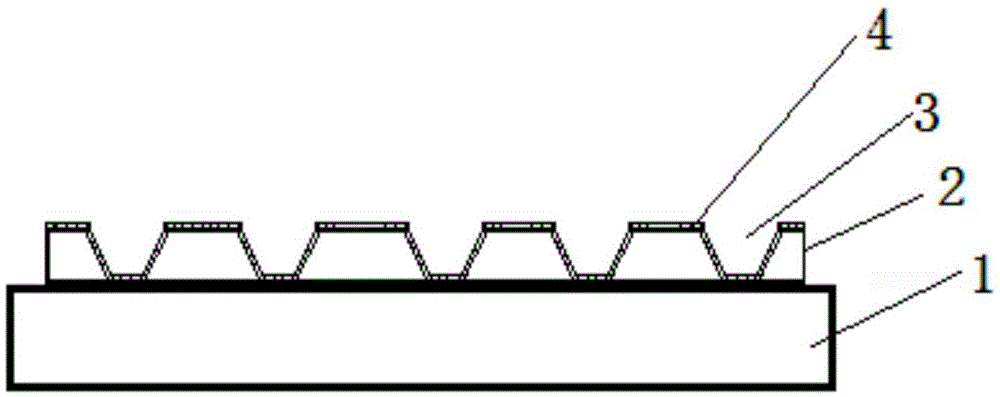
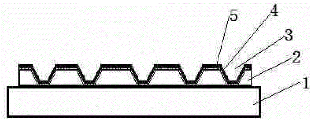
[0029] The present invention proposes an electroless palladium plating method for the through-hole metallization seed layer on the back of the semiconductor, through which palladium ions and reducing agents in a strong acid environment undergo a strong oxidation-reduction reaction with the semiconductor material and the metal surface to replace the palladium on the semiconductor material and the metal surface A layer of palladium seed crystals, and then continuously deposit palladium metal on the palladium seed crystals through the self-excitation of the plating solution in the palladium electroless plating solution, so as to obtain a certain thickness of palladium metal layer on the surface of semiconductor materials and metals to form backside through hole metallization The seed layer is then electroplated on the back of the semiconductor chip that has been electroless palladium plated, and the metallization of the back through hole is completed by using the metal at the botto...


PUM


Abstract

The invention discloses a chemical palladium plating method for a back through hole metallization seed layer of a semiconductor. The chemical palladium plating method comprises the steps: palladium ions and a reducing agent have a strong oxidation-reduction reaction with a semiconductor material and a metal surface in the highly acidic environment, and then a layer of palladium seed crystals is replaced on the semiconductor material and the metal surface; in a palladium chemical plating solution, palladium metal continuously precipitate on the palladium seed crystals by utilizing self-excitation of the plating solution, thereby obtaining a back through hole metallization seed layer formed by a palladium metal layer with a certain thickness on the semiconductor material and the metal surface. Compared with the traditional metal seed layer sputtering technique, the chemical palladium plating method provided by the invention has the advantages of simple process, great technical quality, high yield, wide application range, low costs and the like, and also has excellent market application prospect.

Description

technical field [0001] The invention belongs to the technical field of semiconductor backside technology, and in particular relates to an electroless palladium plating method for a through-hole metallization seed layer on the backside of a semiconductor. Background technique [0002] Back-hole grounding has become a standard process design for GaAs MMICs. It not only reduces the pressure on the front wiring, reduces circuit losses, but also helps to dissipate heat in the active area. At present, the mainstream GaAs MMIC process in the world basically adopts the metallization process module design of sputtering the metal seed layer and then electroplating gold after the back hole is prepared. After years of development, this technology has become mature. The sputtering metal seed layer technology uses the isotropic metallization effect of the sputtering table to sputter the seed layer metal on the back of GaAs and the sidewall of the through hole. [0003] However, in practi...

Claims


Application Information

Patent Timeline
Patent Type & Authority Applications(China)
IPC IPC(8): H01L21/3205C23C18/42C23C18/18C25D7/12
CPCH01L21/32051C23C18/1879C23C18/42C25D7/12
Inventor 邹鹏辉王彦硕潘斌李彭瑞胡俊伟刘鑫
Owner NO 55 INST CHINA ELECTRONIC SCI & TECHNOLOGYGROUP CO LTD
Why Eureka
Try Eureka