Method for improving reliability of SONOS (Semiconductor-Oxide-Nitride-Oxide-Semiconductor) flash memory instrument

A flash memory device, reliability technology, applied in the direction of electric solid-state devices, semiconductor devices, semiconductor/solid-state device manufacturing, etc., can solve problems such as erasing and writing window shrinkage, affecting reliability performance, etc., to achieve easy integration and improve reliability performance , the effect of improving reliability

Inactive Publication Date: 2016-05-04
SHANGHAI HUALI MICROELECTRONICS CORP
View PDF4 Cites 1 Cited by
  • Summary
  • Abstract
  • Description
  • Claims
  • Application Information

AI Technical Summary

Problems solved by technology

The electrons or holes stored in silicon nitride will use this defect chain to escape, thereby making the erasing and writing window extremely narrow, and ultimately affecting the reliability of SONOS devices. Therefore, it is urgent for those skilled in the art to provide a A method for improving the reliability of SONOS flash memory devices, avoiding the phenomenon of electron-hole escape caused by the breakage of silicon-hydrogen bonds in the tunnel oxide layer, and ensuring the data storage capacity of SONOS devices

Method used


Image

  • Method for improving reliability of SONOS (Semiconductor-Oxide-Nitride-Oxide-Semiconductor) flash memory instrument
  • Method for improving reliability of SONOS (Semiconductor-Oxide-Nitride-Oxide-Semiconductor) flash memory instrument
  • Method for improving reliability of SONOS (Semiconductor-Oxide-Nitride-Oxide-Semiconductor) flash memory instrument

Examples


Embodiment 1

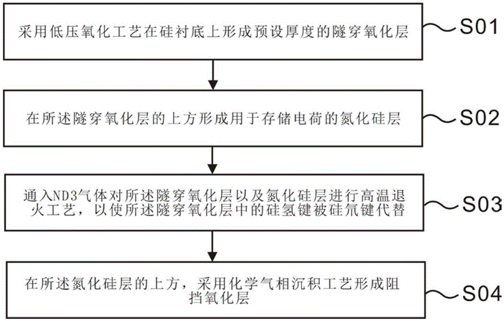
[0035] Such as figure 1 As shown, the present invention provides a kind of method that improves SONOS flash memory device reliability, comprises the following steps:

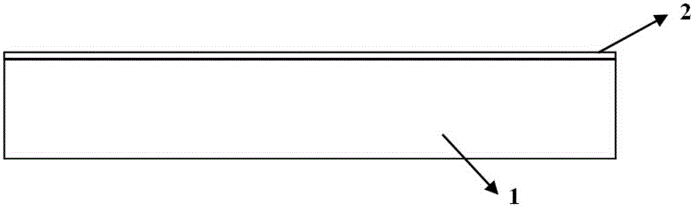
[0036] Step S01, please refer to Figure 3a , forming a tunnel oxide layer 2 with a preset thickness on the silicon substrate 1 by using a low pressure oxidation process.

[0037] Specifically, in this step, it is preferable to use in-situ oxygen atom oxidation equipment to prepare the tunneling oxide layer 2, and the process parameters for preparing the tunneling oxide layer 2 when the in-situ oxygen atom oxidation equipment is: the pressure is 500mtorr to 100torr, and the temperature is 800°C to 1200C, the time is 30s~10min, the ratio of hydrogen to oxygen is 2:1~1:3.

[0038] Step S02, please refer to Figure 3b A high temperature and low pressure chemical vapor deposition process forms a silicon nitride layer 3 for storing charges on the tunnel oxide layer 2 .

[0039] Step S03, please refer to Figure ...

Embodiment 2

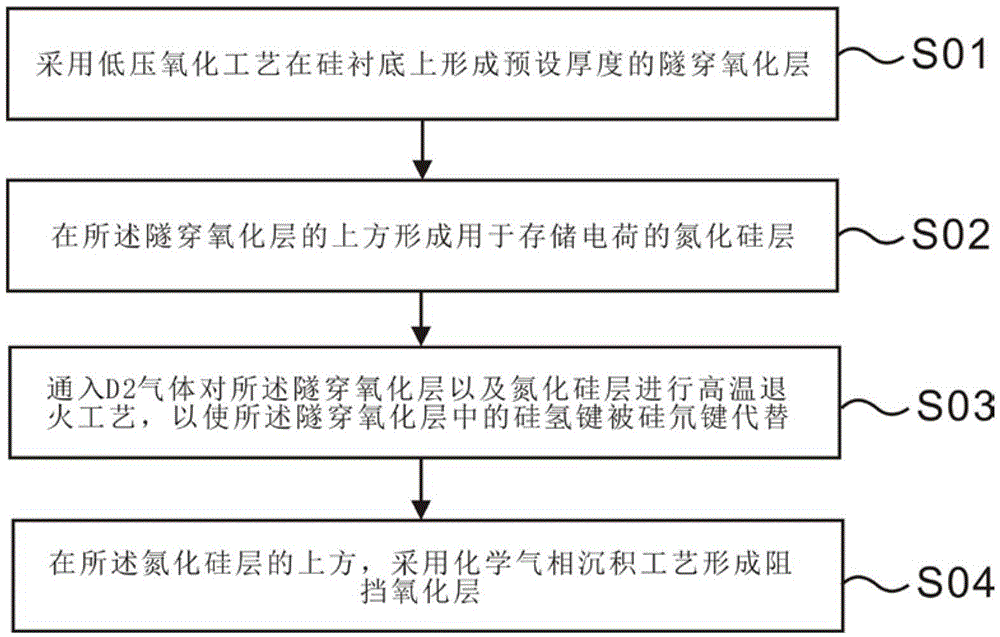
[0044] Such as figure 2 As shown, the present invention also provides a method for improving the reliability of the SONOS flash memory device, comprising the following steps:

[0045] Step S01, please refer to Figure 3a , forming a tunnel oxide layer 2 with a preset thickness on the silicon substrate 1 by using a low pressure oxidation process.

[0046] Step S02, please refer to Figure 3b A silicon nitride layer 3 for storing charges is formed on the tunnel oxide layer 2 by using a high temperature and low pressure chemical vapor deposition process.

[0047] Step S03, please refer to Figure 3c , into D 2 The gas performs a high-temperature annealing process on the tunnel oxide layer 2 and the silicon nitride layer 3, so that the silicon-hydrogen bonds in the tunnel oxide layer are replaced by silicon-deuterium bonds.

[0048] In this step, a high-temperature pre-annealing process is first performed on the tunneling oxide layer 2 and the silicon nitride layer 3, and th...


PUM


Abstract

The invention discloses a method for improving reliability of an SONOS flash memory instrument, comprising following steps: firstly, forming a tunneling oxide layer with a preset thickness and a silicon nitride layer for storing charges on a silicon substrate; then inletting ND3 gas or D2 gas to carrying out a high temperature annealing process to the oxide layer and the silicon nitride layer, causing the silicon-hydrogen bonds in the oxide layer to be replaced by silicon-deuterium bonds; finally forming a barrier oxide layer. According to the method of the invention, the high temperature annealing process is carried out to the oxide layer and the silicon nitride layer; the silicon-hydrogen bonds in the silicon nitride generate fracture; meanwhile, the ND3 gas or D2 gas is inlet; finally the active silicon-hydrogen bonds are replaced by the silicon-deuterium bonds; because the silicon-deuterium bonds are stable, when carrying out a high temperature reliability test, the escaping probability of the electrons is greatly reduced; the reliability of the SONOS instrument is improved; and the method is simple in process, easy in integration and suitable in mass production.

Description

technical field [0001] The invention belongs to the technical field of semiconductor manufacturing and relates to a method for improving the reliability of a SONOS flash memory device. Background technique [0002] SONOS (Semiconductor-Oxide-Nitride-Oxide-Semiconductor) flash memory device has become one of the main flash memory types at present due to its good scaling characteristics and radiation resistance characteristics. There are two main reliability issues faced by SONOS flash memory devices: one is the Endurance (electrical erasing endurance) feature, which measures the possible degradation of SONOS device characteristics after multiple programming / erasing. The second is the DataRetention (data retention) feature, that is, the data retention capability of SONOS devices. [0003] The memory cell of the SONOS flash memory device is composed of an ONO stack structure between the control polysilicon gate and the channel substrate. Among them, the ONO structure consists...

Claims


Application Information

Patent Timeline
Patent Type & Authority Applications(China)
IPC IPC(8): H01L21/8247H01L21/324H01L27/11517H01L27/11551
CPCH01L21/324H10B69/00
Inventor 孙勤
Owner SHANGHAI HUALI MICROELECTRONICS CORP
Why Eureka
Try Eureka