Controllable preparation method of Cu3SbS4 nanocrystalline material

A nanocrystalline material and temperature control technology, applied in the nanomaterials and nano fields, to achieve the effect of simple process, good reproducibility and low cost

Active Publication Date: 2016-05-11
WUHAN UNIV OF TECH
View PDF1 Cites 8 Cited by
  • Summary
  • Abstract
  • Description
  • Claims
  • Application Information

AI Technical Summary

Problems solved by technology

At present, copper antimony sulfur (Cu 3 Sb 4 ) The preparation of nanocrystalline materials is rarely reported, so the study of Cu 3 Sb 4 The preparation process of nanocrystalline materials

Method used


Image

  • Controllable preparation method of Cu3SbS4 nanocrystalline material
  • Controllable preparation method of Cu3SbS4 nanocrystalline material
  • Controllable preparation method of Cu3SbS4 nanocrystalline material

Examples


Embodiment 1

[0019] Cu 3 Sb 4 The controllable preparation method of nanocrystalline material comprises the following steps:

[0020] (1) Add 3mmol cuprous iodide and 1mmol antimony chloride to 10mL oleylamine, pass through argon protection gas, control the temperature at 100°C, and stir rapidly for 20 minutes to make cuprous iodide and antimony chloride Completely dissolve to obtain a complex solution of metal salt;

[0021] (2) Add 11mL, 1mol / L diphenylthiourea diphenyl ether solution to the above metal salt solution, heat to the set temperature of 180°C and react for 120 minutes;

[0022] (3) After the reaction, cool to room temperature, add a large amount of methanol to react the Cu 3 Sb 4 Nanocrystals are cleaned to obtain Cu 3 Sb 4 nanocrystalline material.

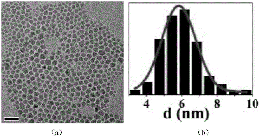
[0023] This embodiment prepares Cu 3 Sb 4 The particle size of the nanocrystalline material is 5.95nm, and its TEM image is shown in figure 2 in a.

Embodiment 2

[0025] Cu 3 Sb 4 The controllable preparation method of nanocrystalline material comprises the following steps:

[0026] (1) Add 3mmol cuprous iodide and 1mmol antimony chloride to 10mL oleylamine, pass through argon protection gas, control the temperature at 80°C, and stir rapidly for 10 minutes to make cuprous iodide and antimony chloride Completely dissolve to obtain a complex solution of metal salt;

[0027] (2) Add 9mL, 1mol / L diphenylthiourea diphenyl ether solution to the above metal salt solution, heat to the set temperature of 120°C and react for 60 minutes;

[0028] (3) After the reaction, cool to room temperature, add a large amount of methanol to react the Cu 3 Sb 4 Nanocrystals are cleaned to obtain Cu 3 Sb 4 nanocrystalline material.

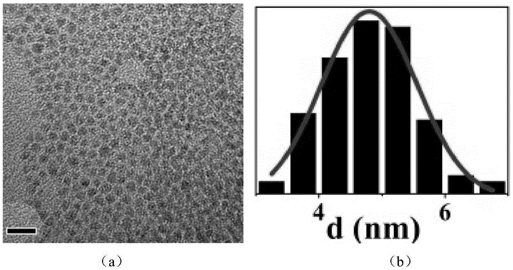
[0029] This embodiment prepares Cu 3 Sb 4 The particle size of the nanocrystalline material is 4.81nm, and its TEM image is shown in image 3 in a.

Embodiment 3

[0031] Cu 3 Sb 4 The controllable preparation method of nanocrystalline material comprises the following steps:

[0032] (1) Add 3mmol cuprous iodide and 1mmol antimony chloride to 10mL oleylamine, pass through argon protection gas, control the temperature at 60°C, and stir rapidly for 5 minutes to make cuprous iodide and antimony chloride Completely dissolve to obtain a complex solution of metal salt;

[0033] (2) Add 7mL, 1mol / L diphenylthiourea solution in diphenyl ether to the above metal salt solution, heat to the set temperature of 60°C and react for 1 minute;

[0034] (3) After the reaction, cool to room temperature, add a large amount of methanol to react the Cu 3 Sb 4 Nanocrystals are cleaned to obtain Cu 3 Sb 4 nanocrystalline material.

[0035] This embodiment prepares Cu 3 Sb 4 The particle size of the nanocrystalline material is 3.37nm, and its TEM image is shown in Figure 4 in a.

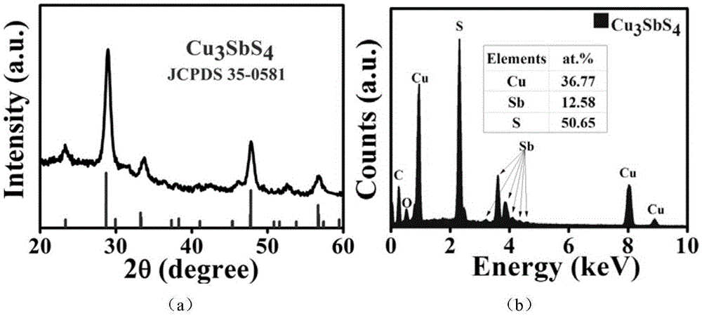
[0036] Cu prepared by the present invention 3 Sb 4 For the XRD spect...


PUM

PropertyMeasurementUnit
Particle sizeaaaaaaaaaa

Abstract

The invention belongs to the field of nano-materials and nano technology and particularly relates to a controllable preparation method of Cu3SbS4 nanocrystalline material, characterized by comprising following steps: 1), adding copper iodide and antimony chloride into oleyl amine according to an addition ratio of 3 mmol:1mmol:10mL for the copper iodide, the antimony chloride and the oleyl amine, introducing protective argon, controlling the temperature and stirring until full dissolution of the copper iodide and the antimony chloride to obtain a metal salt complex solution; 2), adding 7-11 ml of 1mol/L diphenyl ether solution of diphenylthiourea into the metal salt complex solution, and heating to a set temperature and reacting; 3), after reacting is complete, cooling to room temperature, adding methyl alcohol to wash Cu3SbS4 nanocrystalline obtained by reacting to obtain the Cu3SbS4 nanocrystalline material. The preparation method is simple in process and low in cost.

Description

technical field [0001] The invention belongs to the field of nanomaterials and nanotechnology, in particular to a Cu 3 Sb 4 A method for the controllable preparation of nanocrystalline materials. Background technique [0002] Due to the quantum size effect of semiconductor nanocrystalline materials due to their small size, their optical and electrical properties are significantly different from those of their bulk materials, and the differences gradually increase with further reduction in size. This unique property makes semiconductor nanocrystalline materials widely used, such as solar cells, light-emitting diodes, etc. In the past few decades, the research on the synthesis and formation mechanism of semiconductor quantum dots has broadened the types of semiconductor nanocrystalline materials. At present, nanocrystalline materials such as cadmium sulfide, lead sulfide, and copper indium sulfur have been extensively studied and widely used. In recent years, copper antimo...

Claims


Application Information

Patent Timeline
IPC IPC(8): C01G30/00B82Y30/00
Inventor 刘曰利陈克强陈文周静佳丽娜·扎哈若娃
Owner WUHAN UNIV OF TECH
Why Eureka
Try Eureka