Terahertz Spectrum Measurement Device and Measurement Method Based on Scattering Effect

A scattering effect and measurement device technology, applied in the field of spectrum detection, can solve the problems of narrow spectrum measurement range, low resolution, vibration sensitivity, etc., and achieve the effect of wide spectrum restoration range, high resolution and low cost

Active Publication Date: 2018-11-30
NANJING UNIV OF POSTS & TELECOMM
View PDF8 Cites 0 Cited by
  • Summary
  • Abstract
  • Description
  • Claims
  • Application Information

AI Technical Summary

Problems solved by technology

[0008] The technical problem to be solved by the present invention is to overcome the technical problems existing in the prior art such as large volume, high cost, sensitivity to vibration, low resolution, and narrow spectral measurement range, and provide a terahertz sensor based on scattering effect. Spectrum measurement device and terahertz spectrum measurement method

Method used


Image

  • Terahertz Spectrum Measurement Device and Measurement Method Based on Scattering Effect
  • Terahertz Spectrum Measurement Device and Measurement Method Based on Scattering Effect
  • Terahertz Spectrum Measurement Device and Measurement Method Based on Scattering Effect

Examples


Embodiment 1

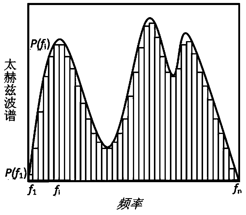
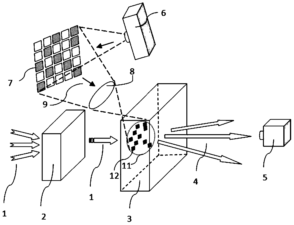
[0071] The structural diagram of the terahertz spectrum measurement device in this embodiment is as follows image 3 shown. In this embodiment, the scattering device 22 is an intrinsic semiconductor 3 whose plasma frequency is lower than the terahertz wave frequency. The intrinsic semiconductor used may be intrinsic gallium arsenide (GaAs) or intrinsic silicon (Si). In this embodiment, the scattering controller 24 is a laser 6, a lens group 8, and a spatial light modulator. The spatial light modulator uses a digital micromirror 7 (Digital Micromirror Device). The laser 6 can be a titanium-doped sapphire laser. The detector 5 is a terahertz wave detector, such as a Golay Cell or a Bolometer. The lens can also be replaced by a reflector. The terahertz wave to be measured passes through the intrinsic semiconductor 3 and the detector 5 sequentially along the transmission direction. The laser 6 , the lens group 8 , and the digital micro-mirror 7 included in the scattering con...

Embodiment 2

[0103] Embodiment 1 is to irradiate the laser beam on the semiconductor surface through the digital micro-mirror 7, so that the irradiated semiconductor surface is arranged with various shapes of laser patterns, so as to realize the function of the scattering controller. In addition to controlling in this way, it is also possible to directly apply different voltages to the laser light source through the power supply of the laser (or modulate it through a stabilized power supply connected to the laser light source), so that the light irradiated on the digital micromirror The laser light intensity changes. But at this time, the switch position of the digital micro-mirror remains unchanged, and the laser pattern irradiated on the surface of the semiconductor does not change. As the light intensity irradiated on the surface of the semiconductor changes, the difference between the dielectric constant of the semiconductor at the irradiated position and the non-irradiated position ch...

Embodiment 3

[0105] The structure of the terahertz spectrum measurement device in this embodiment is as follows Figure 6 and Figure 7 As shown, it includes a terahertz wave collimator 2, an intrinsic semiconductor sheet 3 with a plasma frequency lower than the terahertz wave frequency, a terahertz wave detector 5, a laser 6, etc., at least one surface of the intrinsic semiconductor sheet is rough and uneven of. There are many protrusions or grooves with a line width smaller than one-tenth of the terahertz wavelength on the intrinsic semiconductor rough surface 17 . The protrusions or grooves on the rough surface 17 of the intrinsic semiconductor may be formed by the rough surface of the intrinsic semiconductor material, or by embedding other particulate impurities on the surface of the semiconductor. In order to automatically realize the numerical acquisition and calculation in the spectrum recovery process, the present embodiment also includes a calculation processing unit 25 ( Figu...


PUM


Abstract

The invention discloses a Terahertz spectrum measuring device based on a scattering effect and a measuring method thereof. Terahertz waves to be measured form scattered waves of Terahertz frequency after passing through a scattering device, and the scattered waves are received by a detector under the action of different control conditions of a scattering controller; the scattering device enables the incident Terahertz waves of different frequencies to form different scattered wave intensity angle distributions, and the scattering controller is used for changing scattered field distribution, at the position of the detector, of the Terahertz scattered waves penetrating through the scattering device, so that the scattered waves received by the detector are different in intensity when the incident Terahertz waves of fixed frequency are under the action of different control conditions of the scattering controller; a calculating and processing unit is used for receiving measuring results of the detector and analyzing and processing data. Compared with an existing Terahertz time domain spectrum measuring device, the Terahertz spectrum measuring device has the advantages of being small in size, easy to manufacture, low in cost, high in frequency resolution, wide in spectral measurement range and the like.

Description

technical field [0001] The invention relates to a terahertz spectrum measurement device and a spectrum measurement method, in particular to a device and a spectrum measurement method for spectroscopically measuring a terahertz spectrum through a scattering effect. It belongs to the technical field of spectrum detection. Background technique [0002] As the generation and detection technology of terahertz waves (referring to electromagnetic waves with a frequency range of 0.05-50THz, especially 0.1-10THz) matures, the related technologies and application research of terahertz waves have developed rapidly. Terahertz spectroscopy instrument is one of the most important devices in the field of terahertz wave research. The terahertz spectrum measurement instrument can obtain the terahertz reflection or transmission spectrum of the tested sample, and the obtained terahertz spectrum can be used to identify the composition of the sample, so it can be widely used in many application...

Claims


Application Information

Patent Timeline
Patent Type & Authority Patents(China)
IPC IPC(8): G01N21/49
CPCG01N21/49
Inventor 杨涛黄维朱永元李兴鳌何浩培
Owner NANJING UNIV OF POSTS & TELECOMM
Why Eureka
Try Eureka