Terahertz Spectrum Measuring Device and Its Measurement Method Based on Diffraction Effect

A diffraction effect and measurement device technology, applied in the field of far-infrared detection, can solve the problems of narrow spectral measurement range, low resolution, vibration sensitivity, etc., and achieve the effect of wide spectral restoration range, high resolution and low cost

Active Publication Date: 2018-03-27
南京华睿智光信息科技研究院有限公司
View PDF3 Cites 0 Cited by
  • Summary
  • Abstract
  • Description
  • Claims
  • Application Information

AI Technical Summary

Problems solved by technology

[0007] The technical problem to be solved by the present invention is to overcome the technical problems existing in the prior art such as large volume, high cost, sensitivity to vibration, low resolution, and narrow spectral measurement range, and to provide a terahertz signal based on the diffraction effect. Spectrum measurement device and terahertz spectrum measurement method

Method used


Image

  • Terahertz Spectrum Measuring Device and Its Measurement Method Based on Diffraction Effect
  • Terahertz Spectrum Measuring Device and Its Measurement Method Based on Diffraction Effect
  • Terahertz Spectrum Measuring Device and Its Measurement Method Based on Diffraction Effect

Examples


Embodiment 1

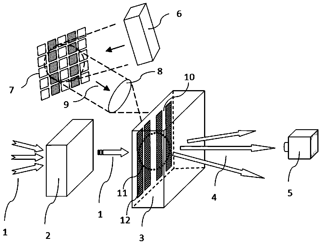
[0063] The structural diagram of the terahertz spectrum measurement device in this embodiment is as follows image 3 shown. In this embodiment, the diffractive device 22 is an intrinsic semiconductor thin slice 3 whose plasma frequency is lower than the terahertz wave frequency. The intrinsic semiconductor used may be intrinsic gallium arsenide (GaAs) or intrinsic silicon (Si). In this embodiment, the diffraction controller 24 is a laser 6, a lens group 8 (which may also be replaced by a mirror), and a spatial light modulator. The spatial light modulator uses a digital micromirror 7 (Digital MicromirrorDevice). The laser 6 can be a titanium-doped sapphire laser. The detector 5 is a terahertz wave detector, such as a Golay Cell or a Bolometer. The terahertz wave to be measured passes through the intrinsic semiconductor 3 and the detector 5 sequentially along the transmission direction. The diffraction controller 24 emits a laser pattern signal to strike the surface of the ...

Embodiment 2

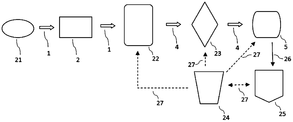
[0096] The structure of the terahertz spectrum measurement device in this embodiment is as follows Figure 6 and Figure 7 As shown, it includes a terahertz wave collimator 2, an intrinsic semiconductor thin film 3 with a plasma frequency lower than the terahertz wave frequency, a metal thin film 17, a terahertz wave detector 5, a laser 6, and the like. In order to automatically realize the numerical acquisition and calculation in the spectrum recovery process, the present embodiment also includes a calculation processing unit 25 ( Figure 6 and Figure 7 not shown). In this embodiment, the diffraction device 22 is composed of one or more diffraction holes or diffraction slits 10 distributed in order or disorderly in the metal thin film 17, which can transmit terahertz waves. The refraction device 23 in this embodiment In this example, it is an intrinsic semiconductor thin slice 3 , and the diffraction controller 24 is a laser 6 and a lens group 8 in this embodiment. The d...

Embodiment 3

[0098] The structure of the terahertz spectrum measurement device in this embodiment is as follows Figure 8 As shown, it includes a terahertz wave collimation device 2, a liquid crystal array and its control system 29, a terahertz wave detector 5, and the like. In order to automatically realize the numerical acquisition and calculation in the spectrum recovery process, the present embodiment also includes a calculation processing unit 25 ( Figure 8 not shown). The diffraction device 22 is composed of a liquid crystal array system 29 capable of modulating terahertz wave transmission in this embodiment, and the diffraction controller 24 is composed of a liquid crystal array controller in this embodiment. Through the control of the liquid crystal array controller, some liquid crystal units in the liquid crystal array have greater transmittance to terahertz waves, while some liquid crystal units have less transmittance to terahertz waves. These liquid crystal units 28 are combi...


PUM


Abstract

The invention discloses a terahertz wave spectrum measurement device and measurement method thereof based on diffraction effect. A to-be-measured terahertz wave forms a terahertz diffracted wave after going through a diffraction device, and the diffracted wave is received by a detector under the force of different control conditions of a diffraction controller. The diffraction device can drive incident terahertz waves of different frequencies to form different diffracted wave intensity angular distributions. The diffraction controller is used to change the diffraction field distribution of the terahertz diffracted wave, passing through the diffraction device, at the position of the detector, so that the detector detects different diffracted wave intensities of the constant frequency incident terahertz wave under the force of the different control conditions of the diffraction controller. A calculation processing unit is used to receive measurement results of the detector and conducts data analysis and processing. Compared with terahertz time-domain wave spectrum measurement devices in the prior art, the device is smaller in size, easier to produce, and lower in cost. The device is high in frequency resolution and wide in spectrum measurement range.

Description

technical field [0001] The invention relates to a terahertz spectrum measurement device and a measurement method thereof, in particular to a diffraction effect-based terahertz spectrum measurement device and a spectrum measurement method, belonging to the technical field of far-infrared detection. Background technique [0002] Terahertz waves (THz waves) or terahertz rays (THz rays) were officially named only in the middle and late 1980s. Before that, scientists would collectively call them far-infrared rays. Terahertz waves generally refer to electromagnetic waves with a frequency in the range of 0.1THz to 10THz, and a wavelength in the range of 0.03mm to 3mm, which is between microwave and infrared waves. The main characteristics of terahertz waves are: (1) terahertz wave photons have low energy and will not cause photodamage and photoionization in biological tissues; (2) because the terahertz spectrum of matter contains rich physical and Chemical information, such as the...

Claims


Application Information

Patent Timeline
Patent Type & Authority Patents(China)
IPC IPC(8): G01J3/18G01J3/28G01J3/02G01N21/3586
CPCG01J3/0229G01J3/18G01J3/28G01N21/3586
Inventor 杨涛黄维何浩培朱永元
Owner 南京华睿智光信息科技研究院有限公司
Why Eureka
Try Eureka