
EUV light source and exposure device

A technology of light source and optical axis, applied in the field of EUV light source and exposure device, can solve the problems of inability to meet production requirements, low power of extreme ultraviolet light, etc., and achieve the effect of increasing power

Active Publication Date: 2016-05-11
SEMICON MFG INT (SHANGHAI) CORP
View PDF6 Cites 4 Cited by
  • Summary
  • Abstract
  • Description
  • Claims
  • Application Information

AI Technical Summary

Problems solved by technology

[0008] However, the power of the extreme ultraviolet light produced by the existing extreme ultraviolet light source is still small, which cannot meet the production requirements

Method used


Image

  • EUV light source and exposure device
  • EUV light source and exposure device
  • EUV light source and exposure device

Examples


Embodiment Construction

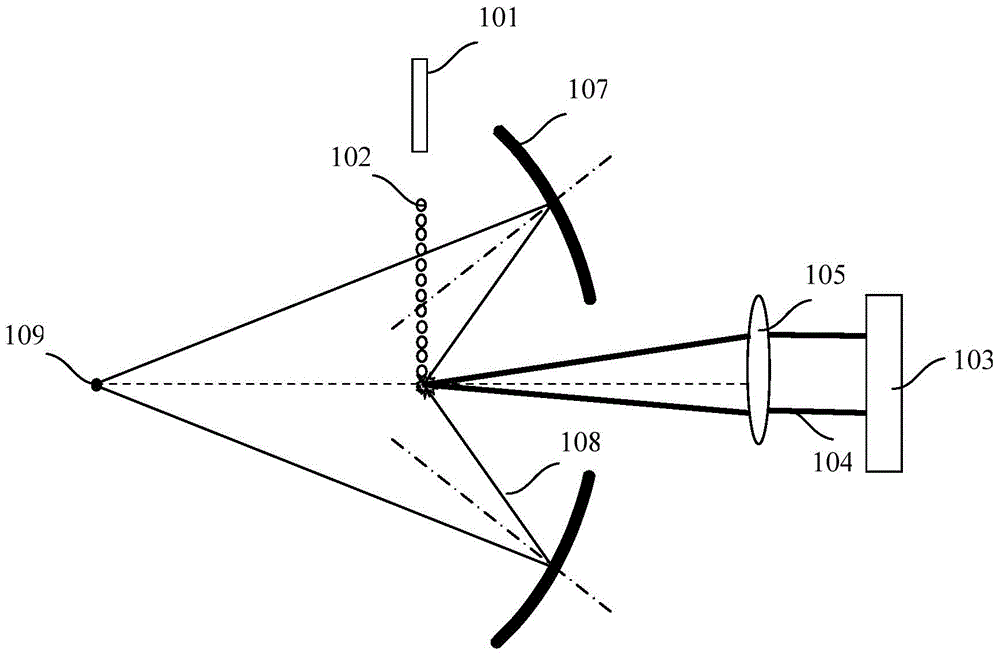
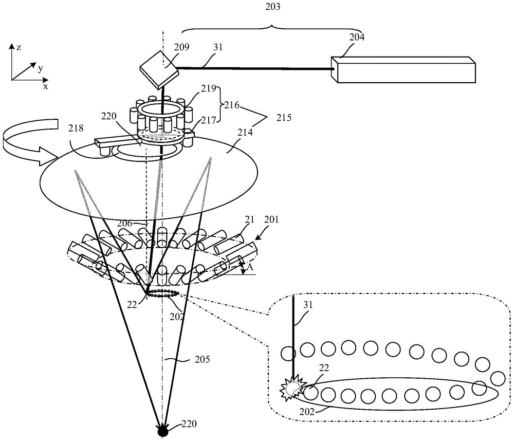
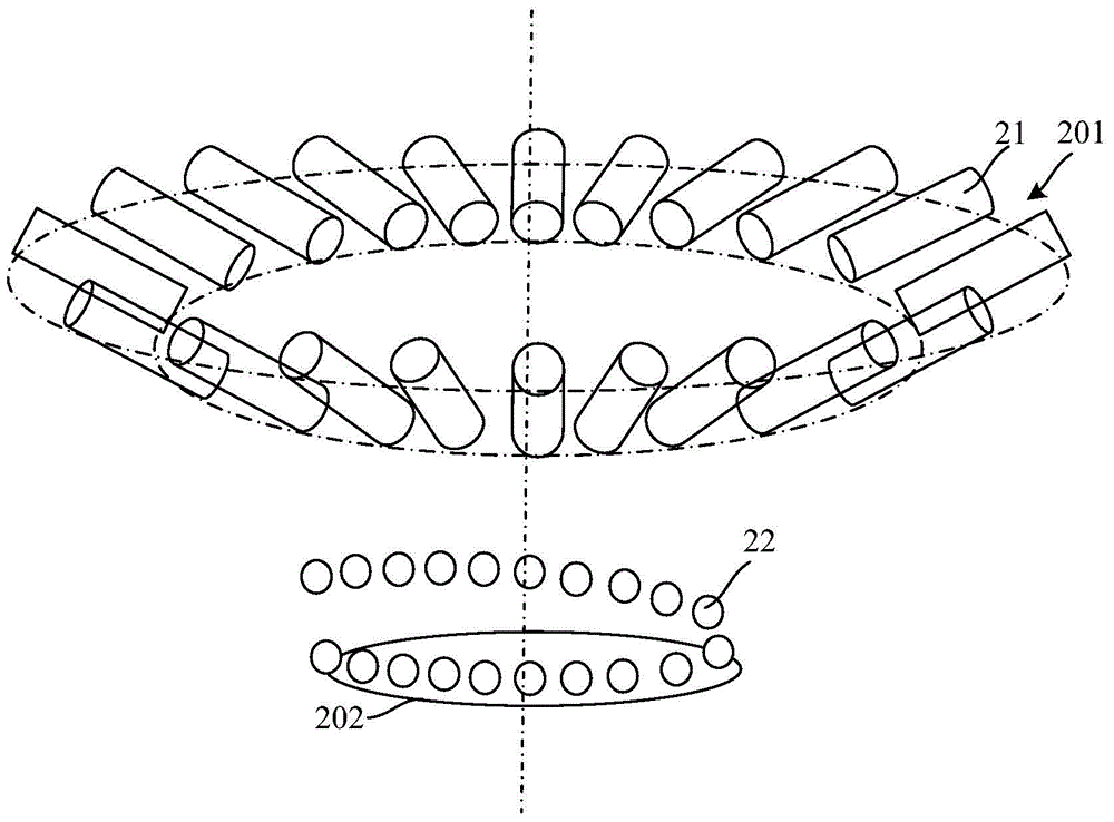
[0036] As mentioned in the background art, the power of the extreme ultraviolet light generated by the existing extreme ultraviolet light source is still small (about 10-30W), and in the actual lithography process, the power of the light source needs to reach 250W. The extreme ultraviolet light source produced by the extreme ultraviolet light source cannot meet the requirements of actual production.

[0037]The study found that the tin droplet nozzle of the existing extreme ultraviolet light source controls the spraying of tin droplets in a mechanical way, so that adjacent tin droplets are separated in space, and the laser beam can bombard each tin droplet. Each tin drop forms plasma when it is bombarded, and the plasma radiation produces extreme ultraviolet light. If the distance between two tin drops is too close or the two tin drops stick together, when the laser beam is bombarding the current tin drop, a The plasma debris will affect the next drop of tin, resulting in poor...


PUM

PropertyMeasurementUnit
Sizeaaaaaaaaaa

Abstract

The invention relates to an EUV light source and an exposure device. The EUV light source comprises a liquid droplet array, a laser source and a light-gathering device, wherein the liquid droplet array comprises a plurality of nozzles which are annularly distributed and sequentially spray liquid droplets to annular radiation positions below the nozzles; the laser source is used for generating laser beams, so that the laser beams sequentially strike liquid droplets reaching the annular radiation positions after being radiated from a position above the liquid droplet array and carrying out rotational scanning, the liquid droplets subjected to laser bombardment form plasmas, and the plasma radiation generates extreme ultraviolet lights; the light-gathering device is positioned above the liquid droplet array, and used for rotationally scanning and collecting the radiated extreme ultraviolet lights, as well as converging the collected extreme ultraviolet lights on a center focus below the annular radiation positions. According to the EUV light source and the exposure device, the power of the extreme ultraviolet lights output by the EUV light source is increased.

Description

technical field [0001] The invention relates to the field of semiconductor fabrication, in particular to an EUV light source and an exposure device. Background technique [0002] Photolithography is an important step in the manufacturing process of semiconductor devices, and this step is to form photolithographic patterns in the photoresist layer using an exposure process and a development process. However, as the integration of chips continues to increase, this requires that the feature size of lithography continues to decrease [0003] The resolution (R) of the exposure device determines the minimum feature size of lithography, and the resolution (R) of the exposure system satisfies the relationship: R=kλ / (NA), where k is a coefficient related to the exposure process, and λ is the exposure The wavelength of the light source, and NA is the numerical aperture of the optical system of the exposure device. It can be known from the foregoing relationship that the resolution o...

Claims


Application Information

Patent Timeline
IPC IPC(8): G03F7/20
Inventor 岳力挽伍强
Owner SEMICON MFG INT (SHANGHAI) CORP
Learn More