
Metal oxide thin film transistor with top gate structure and manufacturing method thereof

A technology of oxide thin film and oxide semiconductor, which is applied in transistors, semiconductor/solid-state device manufacturing, semiconductor devices, etc., can solve the problems of complex overall process and increased production cost, and achieve excellent device performance, low cost, and simple manufacturing process Effect

Inactive Publication Date: 2016-05-11
SOUTH CHINA UNIV OF TECH
View PDF10 Cites 18 Cited by
  • Summary
  • Abstract
  • Description
  • Claims
  • Application Information

AI Technical Summary

Problems solved by technology

[0006] All of the above use the light-shielding layer to block light to avoid damage to the active layer. However, the light-shielding layer must be patterned corresponding to the position of the active layer (especially the channel area), and the area covered by the light-shielding layer must be greater than or equal to the active layer. Only the area of ​​the layer can play a role, especially the channel area, which means at least one more patterning process. The increased patterning process will lead to a complex overall process and increase the production cost.

Method used


Image

  • Metal oxide thin film transistor with top gate structure and manufacturing method thereof
  • Metal oxide thin film transistor with top gate structure and manufacturing method thereof
  • Metal oxide thin film transistor with top gate structure and manufacturing method thereof

Examples


Embodiment 1

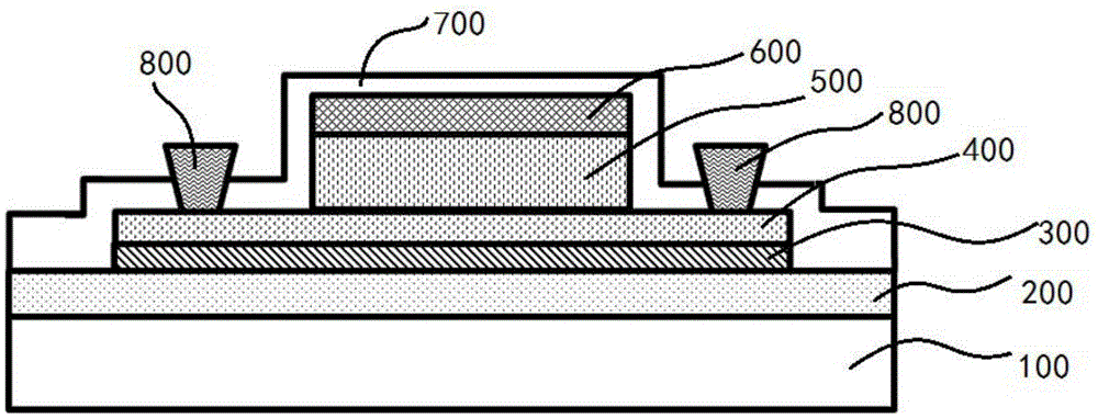
[0036] A metal oxide thin film transistor with a top gate structure, its structure is as follows figure 1 shown. Its preparation method comprises the following steps:

[0037] a. preparing a buffer layer 200 on the substrate 100;

[0038] b. Continuously deposit an opaque insulating light-shielding layer 300 and a metal oxide semiconductor layer on the buffer layer 200, and then pattern the prepared metal oxide semiconductor layer as the active layer 400, while using the patterned metal oxide The semiconductor layer, that is, the active layer 400 is used as a self-aligned pattern to pattern the light-shielding layer 300;

[0039] c. Continuously depositing the first insulating layer and the first metal layer on the active layer 400, then patterning the first metal layer as the gate electrode 600, and then using the patterned gate electrode 600, using a self-alignment method, patterning the first insulating layer as the gate insulating layer 500;

[0040] d. Depositing and ...

Embodiment 2

[0051] A method for preparing a metal oxide thin film transistor with a top gate structure is carried out through the following steps:

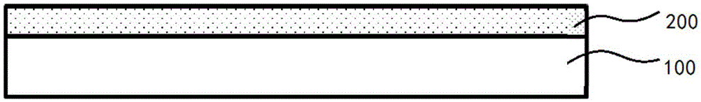
[0052] a. Deposit 300nm SiO on substrate 100 using PECVD 2 As a buffer layer 200, such as figure 2 shown.

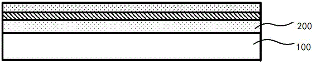
[0053] b. on the buffer layer 200, use the PVD method to continuously deposit the C film of 100nm and the IGZO film of 50nm, such as image 3 shown. Then use HCl with H 2 O ratio is 1:60 dilute hydrochloric acid patterning IGZO thin film obtains active layer 400, then uses N 2 The O gas plasma treatment method uses the active layer 400 as a mask to pattern the C film light-shielding layer 300, such as Figure 4 shown.

[0054] c. Using PECVD method to sequentially deposit 300nm SiO 2 The first insulating layer and the 200nm thick Mo layer are used as the first metal layer, and then the first metal layer is patterned as the gate electrode 600, and then the first insulating layer is patterned by using the self-alignment method wit...


PUM

PropertyMeasurementUnit
thicknessaaaaaaaaaa
thicknessaaaaaaaaaa
thicknessaaaaaaaaaa

Abstract

The invention discloses a method of manufacturing a metal oxide thin film transistor with a top gate structure. The method comprises the following steps: a, a buffer layer is manufactured on a substrate; b, an opaque insulated light shielding layer and a metal oxide semiconductor layer are continuously deposited on the buffer layer, the manufactured metal oxide semiconductor layer is then patterned to serve as an active layer, the metal oxide semiconductor layer after being patterned, that is, the active layer serves as a self-aligned pattern, and the light shielding layer is patterned; c, a first insulated layer and a first metal layer are continuously deposited on the active layer, the first metal layer is then patterned to serve as a gate electrode, and then the patterned gate electrode is used to pattern the first insulated layer to serve as a gate electrode insulated layer by adopting a self-aligned method; d, a second insulated later is deposited and patterned to serve as a passivation layer; and e, second metal layers are deposited on the passivation layer and patterned to serve as source and drain electrodes. The light shielding layer is an amorphous carbon thin film or a hydrocarbon thin film or a diamond-like carbon thin film. The process is simple and the performance is excellent.

Description

technical field [0001] The invention relates to the technical field of semiconductors, in particular to a metal oxide thin film transistor with a top gate structure and a preparation method thereof. Background technique [0002] In recent years, with the rapid development of the new flat panel display (FPD) industry, the thin film transistor (TFT) backplane technology, which is the core technology of FPD, is also undergoing profound changes. Metal Oxide Thin Film Transistor (OTFT) has gradually replaced the traditional amorphous silicon (a-Si) TFT and low temperature polysilicon (LTPS) TFT due to its advantages of high mobility, simple process, low cost, and good uniformity in large area. The new focus of the industry. [0003] However, due to the characteristics of the energy band of the amorphous metal oxide semiconductor material, it is easily affected by light with an energy greater than 2.1eV. These defects limit the use of metal oxide thin-film transistors in liquid ...

Claims


Application Information

Patent Timeline
Patent Type & Authority Applications(China)
IPC IPC(8): H01L21/34H01L29/786
CPCH01L29/66969H01L29/78633H01L29/7869
Inventor 徐苗李民彭俊彪王磊邹建华陶洪
Owner SOUTH CHINA UNIV OF TECH
Learn More