

Technical method of infrared detector indium bump
A technology of an infrared detector and a process method, which is applied in the field of detectors, can solve the problems of unreachable welding, inaccessibility, unevenness, etc., and achieves the effect of solving the problem of flip-chip welding.
- Summary
- Abstract
- Description
- Claims
- Application Information
AI Technical Summary
Problems solved by technology
Method used
Image

Examples
Embodiment Construction
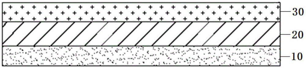
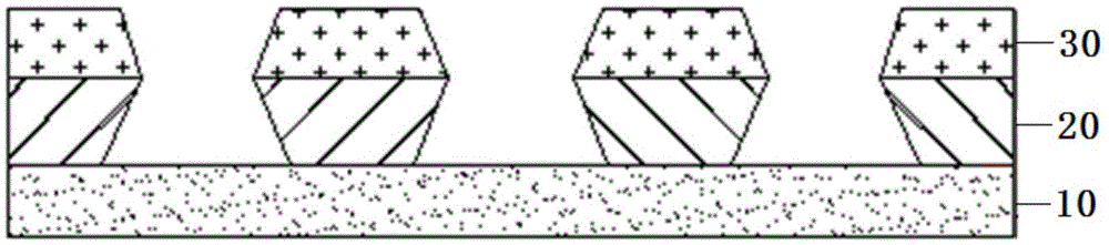
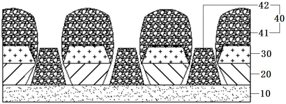
[0018] Embodiments of the present invention are described in detail below, examples of which are shown in the drawings, wherein the same or similar reference numerals designate the same or similar elements or elements having the same or similar functions throughout. The embodiments described below with reference to the accompanying drawings are exemplary, and are only used to explain the technical solution of the present invention, and should not be construed as limiting the present invention.
[0019] In the description of the present invention, the orientation or positional relationship indicated by the terms "inner", "outer", "longitudinal", "transverse", "upper", "lower", "top", "bottom" etc. are based on the drawings The orientations or positional relationships shown are only for the convenience of describing the invention and do not require the invention to be constructed and operated in a specific orientation, and thus should not be construed as limiting the invention. ...
PUM
 Abstract
Description
Claims
Application Information