Shallow-trench half-super-junction VDMOS device and manufacturing method thereof

A manufacturing method and semi-superjunction technology, applied in semiconductor/solid-state device manufacturing, semiconductor devices, electrical components, etc., can solve the problems of weak current conduction per unit area and large forward conduction resistance.

Inactive Publication Date: 2016-05-11
WUXI CHINA RESOURCES HUAJING MICROELECTRONICS
View PDF4 Cites 4 Cited by
  • Summary
  • Abstract
  • Description
  • Claims
  • Application Information

AI Technical Summary

Problems solved by technology

[0009] In view of this, the present invention provides a shallow trench semi-superjunction VDMOS device and a manufacturing method thereof, so as to solve techn

Method used


Image

  • Shallow-trench half-super-junction VDMOS device and manufacturing method thereof
  • Shallow-trench half-super-junction VDMOS device and manufacturing method thereof
  • Shallow-trench half-super-junction VDMOS device and manufacturing method thereof

Examples


Embodiment Construction

[0041] In order to make the above objects, features and advantages of the present invention more comprehensible, specific implementations of the present invention will be described in detail below in conjunction with the accompanying drawings.

[0042] In the following description, many specific details are set forth in order to fully understand the present invention, but the present invention can also be implemented in other ways that are different from those described here, and those skilled in the art can do so without departing from the connotation of the present invention. By analogy, the present invention is not limited by the specific examples disclosed below.

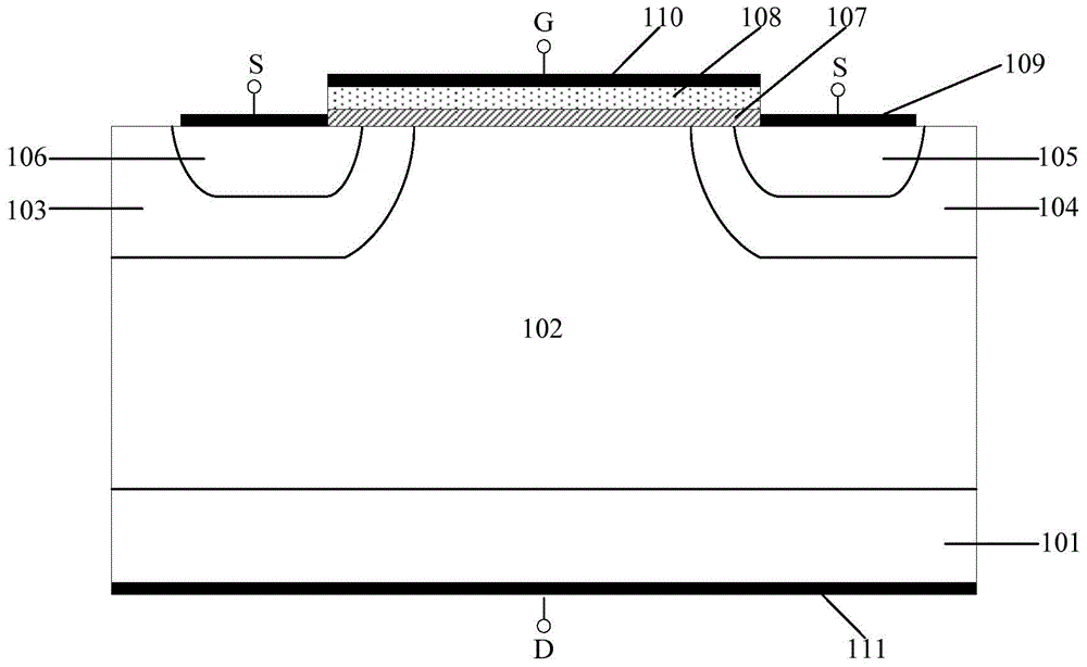
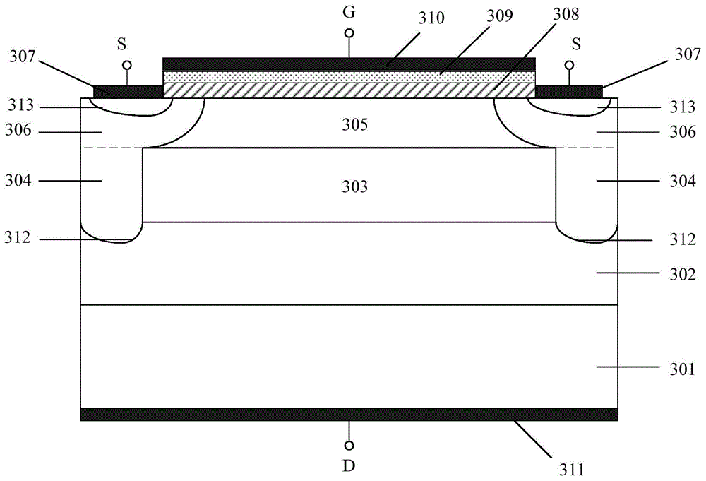
[0043] As mentioned in the background section, the on-resistance of traditional VDMOS is limited by the silicon limit with the growth of withstand voltage, that is, the on-resistance increases rapidly with the increase of withstand voltage, and in order to prevent the resistance region from being broken down, the...


PUM

PropertyMeasurementUnit
Widthaaaaaaaaaa
Depthaaaaaaaaaa

Abstract

The invention discloses a shallow-trench half-super-junction VDMOS device and a manufacturing method thereof. The shallow-trench half-super-junction VDMOS device comprises a first conductive-type substrate, a first resistivity epitaxial layer located above the first conductive-type substrate, a second resistivity epitaxial layer located above the first resistivity epitaxial layer, two third resistivity epitaxial layers and well regions, wherein the third resistivity epitaxial layers are located on two sides of an upper surface of the second resistivity epitaxial layer and are extended to two groove areas of a bottom of the second resistivity epitaxial layer from the upper surface; the third resistivity epitaxial layers of a second conductive type is generated in grooves; the well regions are injected from two sides of an upper surface of a fourth resistivity epitaxial layer and are connected to the third resistivity epitaxial layers in the two grooves. In the invention, process flow cost is considered and manufacturing is convenient; and because of existence of a half-super-junction structure, a forward conduction resistance of the VDMOS device is greatly reduced and a unit area current conduction capability is high.

Description

technical field [0001] The invention relates to the technical field of semiconductor devices and manufacturing techniques thereof, in particular to a shallow trench semi-superjunction VDMOS device and a manufacturing method thereof. Background technique [0002] VDMOS (VerticalDouble-diffused MetalOxideSemiconductor, vertical double-diffused metal oxide semiconductor) device is a power semiconductor device that has the advantages of both bipolar transistors and ordinary MOS devices. Compared with bipolar transistors, it has fast switching speed, small switching loss, high input impedance, low driving power, good frequency characteristics, high transconductance linearity, no secondary breakdown problem of bipolar power devices, and safe The work area is large. Therefore, VDMOS devices are ideal power semiconductor devices for both switching and linear applications. [0003] For VDMOS devices, one of its important indicators is the on-resistance. With the development of VDM...

Claims


Application Information

Patent Timeline
IPC IPC(8): H01L29/78H01L29/06H01L21/336
CPCH01L29/0878H01L29/0634H01L29/66712H01L29/7802
Inventor 周宏伟阮孟波孙晓儒
Owner WUXI CHINA RESOURCES HUAJING MICROELECTRONICS
Why Eureka
Try Eureka