A kind of preparation method of single-layer nanometer resistive film memristor

A memristor and nano-film technology, applied in the field of nonlinear circuit applications, can solve the problems of long preparation period, high requirements, complex preparation process, etc., and achieve the effects of easy physical realization, improved resistance performance, and simple preparation process

Active Publication Date: 2018-02-06
SHANDONG UNIV OF SCI & TECH
View PDF5 Cites 0 Cited by
  • Summary
  • Abstract
  • Description
  • Claims
  • Application Information

AI Technical Summary

Problems solved by technology

[0005] (1) In recent years, new memristor materials and memristor systems have been continuously reported, but there are still few physically realized memristor models, and they are relatively single, and there is no unified universal model to describe the behavior of memristors
[0006] Most of the physical memristors reported in recent years are proposed for certain types of applications or for simulating certain functions (such as high-density non-volatile memory, Crossbar Latch technology, and simulated synapses). The similar switch model and working mechanism, and the manufacturing process is complicated and the cost is high. It is not general and universal for the study of memristor characteristics, memristor circuit theory and electronic circuit design.
[0007] (2) Commercial production has not yet been realized
[0008] It is difficult for most researchers to obtain a real memristor element, so many researchers cannot carry out hardware experiments in the real physical sense due to the lack of memristor elements when studying memristors and memristor circuits. Rely on simulation or simulated circuits for experimental research
However, the memristor simulation model and the analog circuit are far from the actual memristor characteristics, and the hardware implementation using the analog circuit is more concerned with simulating the memristor mathematical model and ignoring the essential physical characteristics of the memristor
[0009] (3) The preparation of physical memristors that have been reported requires high requirements and harsh conditions in terms of raw material selection and preparation process methods, and it is difficult for laboratories or scientific research units with ordinary conditions to complete the preparation of related physical memristor components.
[0016] 2. The preparation process is complicated, the preparation cycle is long, and the energy consumption is high:
[0018] In addition, it also has the problems and deficiencies of relatively harsh process conditions and low product rate.

Method used


Image

  • A kind of preparation method of single-layer nanometer resistive film memristor
  • A kind of preparation method of single-layer nanometer resistive film memristor
  • A kind of preparation method of single-layer nanometer resistive film memristor

Examples


Embodiment 1

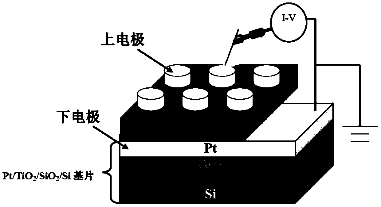
[0091] The preparation method of the memristor comprises the following steps:

[0092] The first step is to prepare Bi (1-x) Ca x FeO 3-x / 2 The mixture target, the specific steps are as follows:

[0093] (1), mixing of raw materials:

[0094] will Bi 2 O 3 : CaCO 3 : Fe 2 O 3 =99:2:100 (molar ratio) mixing;

[0095] Add deionized water or anhydrous ethanol, and grind into a mill until the particle size is below 0.08mm;

[0096] Take out and dry to obtain a mixture;

[0097] (2), granulation:

[0098] The above mixture is granulated: according to 2-5% of the mass of the mixture to be granulated, a polyvinyl alcohol solution with a mass percentage concentration of 2-5% is added, and after mixing evenly, granulation is carried out through a 40-mesh sieve;

[0099] (3), Bi (1-x) Ca x FeO 3-x / 2 Compression molding of mixture targets:

[0100] The granulated material is placed on a tablet press and pressed into a block; then, the obtained block material is cut into d...
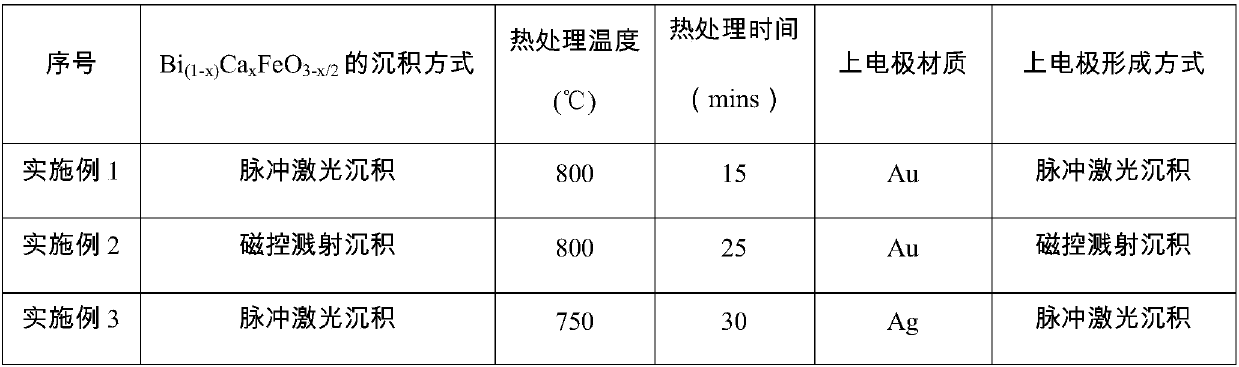
Embodiment 2

[0109] In addition to preparing Bi (1-x) Ca x FeO 3-x / 2 The raw material formula of the mixture target is: Bi 2 O 3 : CaCO 3 : Fe 2 O 3 = 98:4:100 (molar ratio), and in addition to the parameters in Table 1 below;

[0110] The rest are the same as in Example 1.

Embodiment 3

[0112] In addition to preparing Bi (1-x) Ca x FeO 3-x / 2 The raw material formula of the mixture target is: Bi 2 O 3 : CaCO 3 : Fe 2 O 3 = 97:6:100 (molar ratio), and in addition to the parameters in Table 1 below;

[0113] The rest are the same as in Example 1.


PUM


Abstract

The invention discloses a preparation method of a single-layer nano-resistive film memristor, which uses the holes and ionized oxygen ions generated by the single-layer nano-film memristor under bias voltage as carriers, relying on the holes and ionization The principle of changing the resistance of the device by changing the amount of oxygen ions generated is based on the existing technology, starting from the simplification of the preparation process and the chemical formula of the resistive film nano-ceramic material. The sintering step, the selection of raw materials with higher valence of metal cations and lower sintering temperature of nano-ceramic, combined with lower calcination temperature to control it into an incomplete "sintering", thereby greatly increasing its internal lattice defects and voids. A series of technical means such as holes simplifies the preparation process, shortens the process flow, improves production efficiency, and reduces production energy consumption and manufacturing costs; at the same time, the memristor performance and yield of memristors are greatly improved.

Description

technical field [0001] The invention relates to a preparation method of a memristor, in particular to a preparation method of a single-layer nanometer resistive variable film memristor, and belongs to the field of nonlinear circuit application. Background technique [0002] Memristors, also known as memristors, are the fourth type of passive circuit element to appear after resistors, capacitors, and inductors. Due to its non-volatile, synaptic function and nanoscale structure, it is widely used in high-density non-volatile memory, artificial neural networks, large-scale integrated circuits, reconfigurable logic and programmable logic, bioengineering, pattern recognition, signal Processing and other fields have huge application prospects. And it is expected to pave the way for the manufacture of non-volatile memory devices with unlimited storage accuracy and ultra-high storage density, artificial neural networks that can adjust the synaptic weight of neurons, and analog comp...

Claims


Application Information

Patent Timeline
Patent Type & Authority Patents(China)
IPC IPC(8): H01L45/00B82Y30/00B82Y40/00
CPCB82Y30/00B82Y40/00H10N70/041H10N70/026
Inventor 窦刚郭梅李玉霞孙钊李煜于洋
Owner SHANDONG UNIV OF SCI & TECH
Why Eureka
Try Eureka