Small differential notch UWB-MIMO antenna
A wave trap and antenna technology, applied in the field of wireless mobile communication, can solve the problems of reducing system efficiency, increasing the number of independent devices, not conducive to high integration and miniaturization of the system, and achieving good impedance matching, reducing size, and increasing isolation. Effect
- Summary
- Abstract
- Description
- Claims
- Application Information
AI Technical Summary
Problems solved by technology
Method used
Image
Examples
Embodiment 1
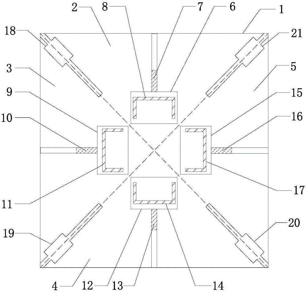
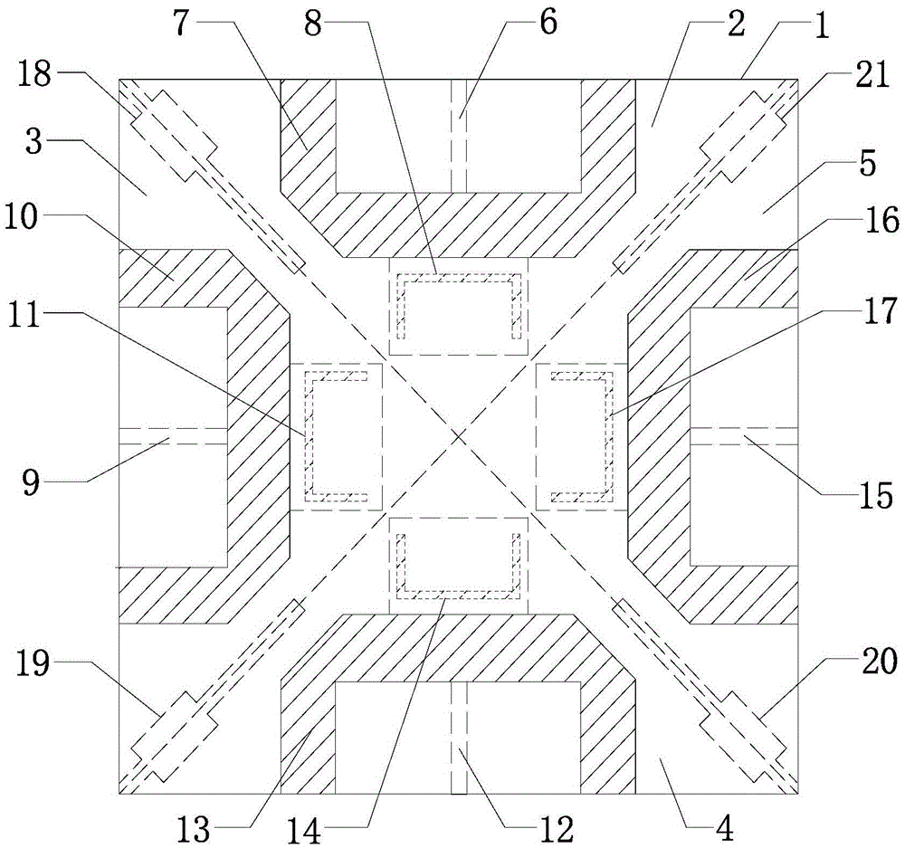
[0033] Such as figure 1 with figure 2 As shown, the UWB-MIMO antenna of this embodiment includes a dielectric substrate 1, a floor arranged on the top layer of the dielectric substrate 1, and four quadrilaterals separated by a pair of diagonal lines on the top layer of the dielectric substrate 1 and a pair of diagonal lines on the bottom layer of the dielectric substrate 1. An antenna unit, the floor is etched with four symmetrical slits on a pair of diagonal lines on the top layer of the dielectric substrate 1, and the four antenna units are separated by four slits, which can improve the distance between the four units isolation;
[0034] The four antenna units are respectively the first antenna unit 2, the second antenna unit 3, the third antenna unit 4 and the fourth antenna unit 5; the first antenna unit 2 includes a first T-shaped antenna etched on the floor The slot 6 and the first differential feed structure 7 arranged on the bottom layer of the dielectric substrate ...
Embodiment 2
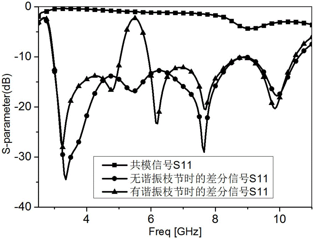
[0041] The dielectric substrate 1 adopted in this embodiment is an FR4 dielectric substrate, and its dielectric constant ε e =4.4, thickness d=1.6mm, the floor is printed on the top layer of the dielectric substrate 1, and the differential feeding part is printed on the bottom layer of the dielectric substrate 1; the structures of the four antenna elements are basically the same, and the arrangement in this way can greatly reduce the size of the antenna, In each antenna unit, the differential signal is fed from P+ (P1+, P2+, P3+, P4+) and P- (P1-, P2-, P3-, P4-), and the T-shaped slot is fed through the differential feeding structure. The differential feed structure is composed of microstrip feeders, and it is designed in the form of chamfered corners, which can realize ultra-wideband operation; the vertical placement of the differential feed structure and the T-shaped slot makes it impossible for the common-mode signal to excite the slot, and the common-mode signal can be cert...
PUM
 Abstract
Description
Claims
Application Information


