A single-event upset-resistant latch with low delay power product

An anti-single-event, latch technology, applied in the field of latches against single-event flip, can solve the problems of latch flip, circuit high power consumption delay product hardware overhead, large hardware overhead, etc., to speed up writing speed, improving the ability of anti-single-event flipping, and the effect of good anti-single-event flipping ability

Active Publication Date: 2018-06-26
XI AN JIAOTONG UNIV
View PDF2 Cites 0 Cited by
  • Summary
  • Abstract
  • Description
  • Claims
  • Application Information

AI Technical Summary

Problems solved by technology

DICElatch proposed by T.Calin and M.Nicolaids (T.Calin, M.Nicolaids, R.Velazco, 1996, IEEE Transactions on Nuclear Science, 43, p2874.) has good anti-single event flipping ability, and the critical charge of its key nodes is much larger than that of traditional The latch, but requires a lot of hardware overhead, such as large-size transistors
FERSTlatch proposed by M.Fazeli and S.G.Miremadi et al. (M.Fazeli, S.G.Miremadi, A.Ejlali, A.Patooghy, 2009, Computers & Digital Techniques, 3, p289.) Its internal nodes have a good ability to resist single event effects, however , if the injected particle energy is strong enough, the external output node of the latch also has a great risk of flipping, and the circuit also has a large power consumption delay product and a certain hardware overhead

Method used


Image

  • A single-event upset-resistant latch with low delay power product
  • A single-event upset-resistant latch with low delay power product
  • A single-event upset-resistant latch with low delay power product

Examples


Embodiment Construction

[0018] The present invention is described in further detail below in conjunction with accompanying drawing:

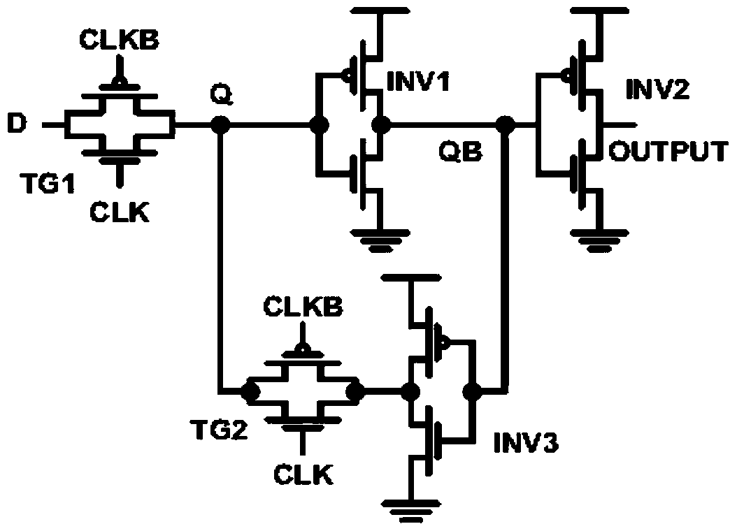
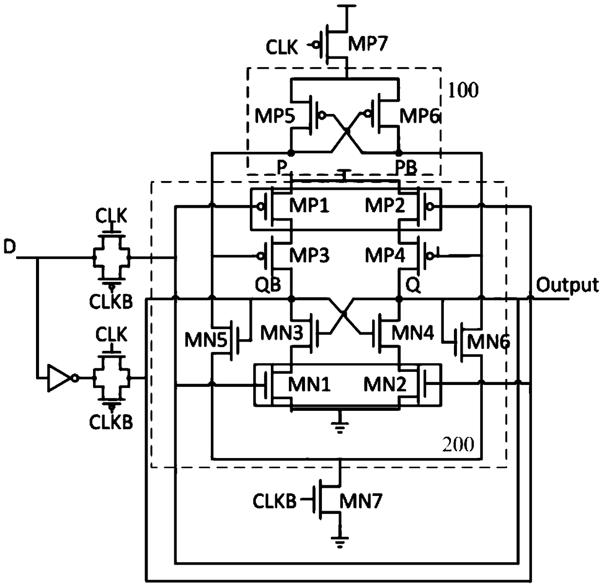
[0019] see figure 1 and figure 2 , the present invention is based on the traditional latch (such as figure 1 As shown), two cross-coupled transistors are used to form a negative feedback path to speed up the recovery speed of the flipped sensitive node. The entire anti-radiation D latch circuit has four external ports, two input ports (D, CLK), and two complementary output ports (Q, QB).

[0020] Add four redundant transistors (MP1, MP2, MN1, MN2), when the latch is working in the normal data writing stage, the four transistors controlled by the storage nodes Q and QB will be turned off, thus cutting off the negative circuit. The feedback path can effectively block the interference of the negative feedback path to data writing, and improve the writing speed of the circuit. When the circuit works in the latched state, the node flipping state caused by the single ev...


PUM


Abstract

The invention discloses an anti-single-event-upset latch register with a low delay-power product. By use of a novel cross coupling structure capable of isolating an upset state, recovery of the upset state is accelerated through design of a reasonable negative feedback passage. In case of a data transparent mode, negative feedback is cut off so as to improve the writing speed of a circuit. A simulation result under a 40nm CMOS technology shows that the critical charge ratio of the latch register provided by the invention is more than 50 times higher than that of a conventional latch register. The delay-power product is only 0.0035fs*J, and the propagation time delay under the non-loaded condition is only 23.3ps, which is lower than that of a same-type latch register.

Description

【Technical field】 [0001] The invention belongs to the technical field of integrated circuits, and in particular relates to a novel anti-single event reversal latch with low delay power consumption product. 【Background technique】 [0002] With the advancement of integrated circuit manufacturing technology, the feature size of CMOS devices has reached the nanometer level, and the power supply voltage and node critical charge of digital circuits are also decreasing, making them more and more vulnerable to soft damage caused by single event effects (SEU). The effect of errors. Especially for a latch or flip-flop, once its internal node is affected by a single event, it will cause the latch state to flip, resulting in the destruction of the stored signal. Single event effects have become a major source of soft errors in digital integrated circuits. For digital memory chips used in special fields (aerospace, military industry, etc.), it is necessary to carry out anti-radiation h...

Claims


Application Information

Patent Timeline
Patent Type & Authority Patents(China)
IPC IPC(8): H03K3/3565H03K3/012H03K3/013
CPCH03K3/012H03K3/013H03K3/3565
Inventor 张国和陈云王丽段国栋
Owner XI AN JIAOTONG UNIV
Why Eureka
Try Eureka