
Linear optical signal storage method for single-photon avalanche diode

A single-photon avalanche and linear storage technology, applied in image communication, color TV parts, TV system parts, etc., can solve the constraints of SPAD pixel resolution performance, low sensor integration, large unit pixel area, etc. problem, to achieve high integration, improve pixel integration, and increase the effect of duty cycle

Inactive Publication Date: 2016-05-11
苏州超锐微电子有限公司
View PDF2 Cites 2 Cited by
  • Summary
  • Abstract
  • Description
  • Claims
  • Application Information

AI Technical Summary

Problems solved by technology

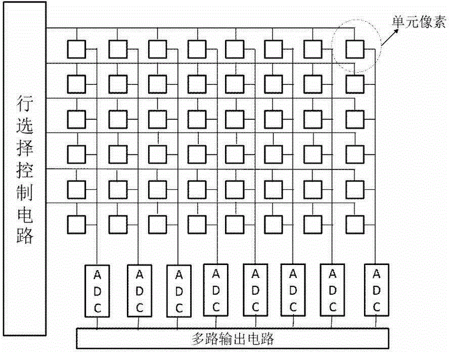
However, since each pixel contains a huge circuit module, the final unit pixel area is too large, resulting in low integration and low resolution of the sensor.
This also restricts the pixel resolution performance of SPAD as an imaging sensor

Method used


Image

  • Linear optical signal storage method for single-photon avalanche diode
  • Linear optical signal storage method for single-photon avalanche diode
  • Linear optical signal storage method for single-photon avalanche diode

Examples


Embodiment Construction

[0023] The invention will be described in further detail below in conjunction with the accompanying drawings.

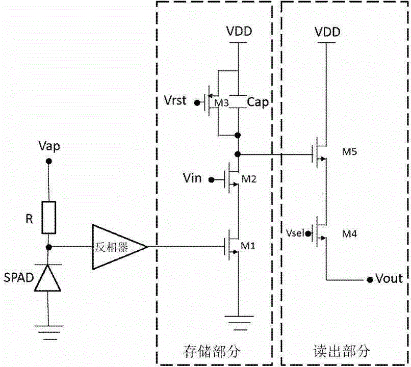
[0024] Such as figure 1 As shown, the single photon avalanche diode (SPAD) cathode applies a forward bias voltage Vap to make the SPAD work in Geiger mode:

[0025] (1) Reset stage: Before optical signal detection, bias the Vrst voltage to make the MOS transistor M3 turn on, bias the Vin voltage to make the MOS transistor M2 turn off, and charge the capacitor Cap to the power supply voltage VDD;

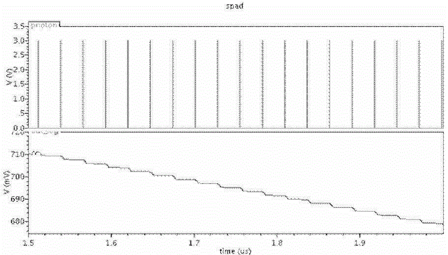
[0026] (2) Optical signal storage stage: Bias the Vrst voltage to make the MOS tube M3 turn off, bias the Vin voltage to make the MOS tube M2 turn on, and the SPAD starts to perform photoelectron detection. When the SPAD detects a photon signal, an avalanche will occur, and a large pulse current will be generated. Due to the voltage division effect of the resistor R, the voltage on the diode will decrease, and the inverter will output a high voltage pulse to turn on the M1...


PUM


Abstract

The invention provides a novel storage method for an optical signal, wherein the single-photon detection capability of the single-photon avalanche diode is used. The method includes three continuous processes of signal storage, reading out, and resetting. At the storage stage, when a single-photon avalanche diode detects a photon signal, a current and voltage pulse signal is generated; and an MOS tube M1 is opened by the signal, so that discharging of a capacitor is carried out by one time. At the reading out stage, the voltage value of the capacitor can be read out by a source follower, thereby obtaining a corresponding detected photon number. After completion of the reading out stage, an MOS tube M3 is opened, so that the capacitor is charged to be at the power voltage, thereby realizing resetting.

Description

technical field [0001] The invention relates to the field of single-photon detectors, in particular to a method for linearly storing optical signals based on single-photon avalanche diodes, which can realize linearly storing and reading optical signals. Background technique [0002] In recent years, solid-state digital image sensor technology has been developed rapidly. Solid-state digital image sensor technology currently mainly includes charge-coupled device technology (ChargeCoupledDevice, referred to as CCD) and CMOS image sensor technology (CMOSActivePixelSensor, referred to as CMOS-APS). Especially since the beginning of the 21st century, with the development of standard integrated circuit technology towards the nanometer level, CMOS-APS technology has achieved more advanced development, and has completely surpassed CCD in terms of integration, power consumption and cost, and has become the mainstream. consumer technology. [0003] However, with the development of lo...

Claims


Application Information

Patent Timeline
Patent Type & Authority Applications(China)
IPC IPC(8): H04N5/3745H04N5/378
Inventor 卜晓峰沈寒冰朱小茅吴俊辉
Owner 苏州超锐微电子有限公司
Learn More