Novel lamination structure of multilayer high-speed PCB and signal via-hole optimization method

A stacked structure, signal via technology, applied in the reduction of crosstalk/noise/electromagnetic interference (, circuit devices, conductive pattern layout details, etc., can solve the problem of signal via impedance discontinuity, etc., to achieve good service product design , The effect of improving SI performance

Inactive Publication Date: 2016-05-11
SYSU CMU SHUNDE INT JOINT RES INST +1
View PDF15 Cites 12 Cited by
  • Summary
  • Abstract
  • Description
  • Claims
  • Application Information

AI Technical Summary

Problems solved by technology

[0005] The stacked structure provided by the present invention is used to solve the signal integrity problem caused by the impedance discontinu

Method used


Image

  • Novel lamination structure of multilayer high-speed PCB and signal via-hole optimization method
  • Novel lamination structure of multilayer high-speed PCB and signal via-hole optimization method
  • Novel lamination structure of multilayer high-speed PCB and signal via-hole optimization method

Examples


Embodiment 1

[0032] The invention provides a novel multi-layer high-speed PCB laminate design and proposes a multi-layer high-speed PCB signal via optimization method with wide applicability on the basis of the laminate.

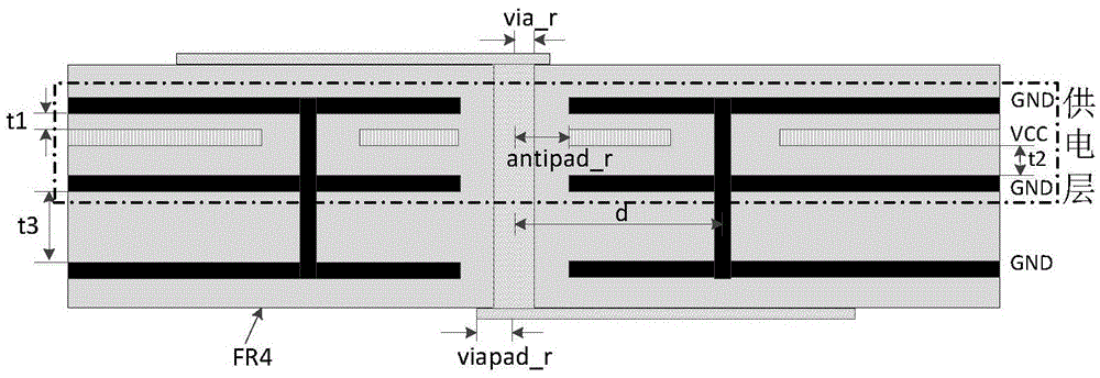
[0033] The main feature of the high-speed multi-layer PCB stacking scheme provided by the present invention is that all power planes are only used for power supply, each power plane is sandwiched by two ground planes with a thin medium, and all signal layers are separated by ground planes , so that each signal layer has a good reference plane, and four short-circuit holes (ground holes) are evenly placed around the signal via hole to provide a low-impedance return path for the signal via hole.

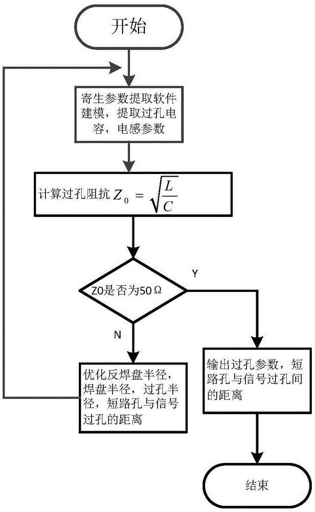
[0034] On the basis of this stack, by optimizing the parameters such as pad radius, via hole radius, anti-pad radius, and the distance from the short-circuit hole to the signal via hole, a performance optimization scheme for signal vias is proposed through repeated iterative optim...

Embodiment 2

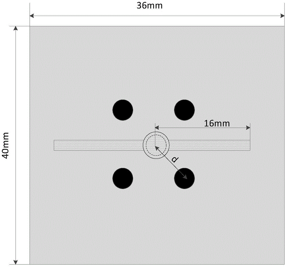
[0040] The schematic diagram of the laminate of the multilayer high-speed PCB proposed in this embodiment is as follows: figure 1 , 2 As shown, place four short-circuit holes (ground holes) evenly around the signal via hole. figure 1 The lamination thicknesses in are respectively: t1=0.05mm, t2=0.1mm, t3=1mm. First, follow the figure 1 The stackup schematic is shown as well as Figure 4 The size of the top view is shown to establish a three-dimensional parasitic parameter extraction model. The size of the PCB in the established three-dimensional parasitic parameter extraction model is: 18mm*20mm, and the length of the microstrip line is: 1mm. Set the solution frequency to 5GHz, repeatedly optimize parameters such as pad radius, via hole radius, anti-pad radius, distance from short-circuit hole to signal via hole, and iteratively optimize, according to the characteristic impedance calculation formula Calculate impedance. After actual calculation and optimization, on the b...


PUM

PropertyMeasurementUnit
Thicknessaaaaaaaaaa
Radiusaaaaaaaaaa
Radiusaaaaaaaaaa

Abstract

The invention relates to a novel lamination structure of a multilayer high-speed PCB. The novel lamination structure comprises multiple layers of ground planes, power supply planes arranged between every two adjacent ground planes, and two layers of signal planes arranged on the top layer and the bottom layer of a PCB, which are up-down successively arranged. Spaces between the power supply planes and adjacent two layers of ground planes are filled with medium. Each of the signal planes arranged on the top layer and the bottom layer of the PCB comprises a weld disc and a microstrip line. A signal via hole is arranged in each of the weld discs. The microstrip lines are connected together via the signal via holes. N grounding short circuit holes are uniformly arranged around each of the signal via hole. According to the invention, the grounding short circuit holes can provide ideal low-impedance returning paths for the signal via holes, and parasitic parameters of current paths among the planes are reduced.

Description

technical field [0001] The invention relates to the field of signal via impedance consistency control, and more specifically, relates to a novel laminated structure of a multilayer high-speed PCB and a signal via hole optimization method. Background technique [0002] With the development of semiconductor technology towards high speed and high density, the speed and bandwidth of high-speed PCB interconnection system are getting bigger and bigger, and the signal integrity problems caused by it are getting more and more serious. The signal integrity problem of high-speed PCB directly restricts the performance of the product, and is also a key issue in the actual product design process. Now most of the communication equipment is the so-called high-density interconnect (HDI) system, and the functions integrated on the PCB board More and more, the layout and wiring density is quite large, and the signal integrity problem faced is more severe. The application of high-speed serdes ...

Claims


Application Information

Patent Timeline
IPC IPC(8): H05K1/02
CPCH05K1/0216H05K1/0298H05K2201/093
Inventor 张木水黄鹏
Owner SYSU CMU SHUNDE INT JOINT RES INST
Why Eureka
Try Eureka