
MEMS device, preparation method and electronic apparatus

A technology of electronic devices and devices, which is applied in the field of MEMS devices and their preparation, can solve problems such as device preparation difficulties, and achieve the effect of strong implementability and low cost

Active Publication Date: 2016-05-18
SEMICON MFG INT (SHANGHAI) CORP
View PDF6 Cites 4 Cited by
  • Summary
  • Abstract
  • Description
  • Claims
  • Application Information

AI Technical Summary

Problems solved by technology

It is necessary to control the arc-shaped morphology formed during the photolithography process, but the arc-shaped photoresist morphology in the existing method is uncontrollable, which brings difficulties to the preparation of the device

Method used


Image

  • MEMS device, preparation method and electronic apparatus
  • MEMS device, preparation method and electronic apparatus
  • MEMS device, preparation method and electronic apparatus

Examples


preparation example Construction

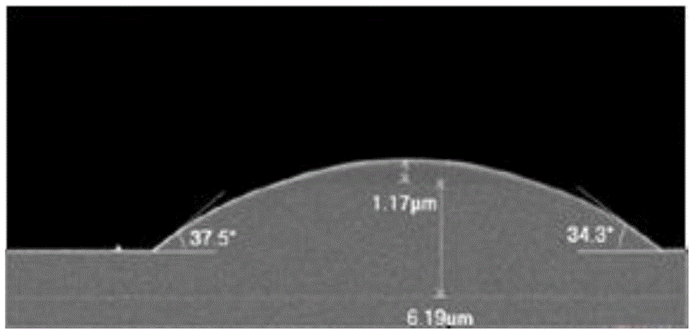
[0039] Arc-shaped steps are often used in the preparation process of MEMS devices, such as Figure 1c shown. Usually, the following two methods are used to change the pattern morphology after photolithography:

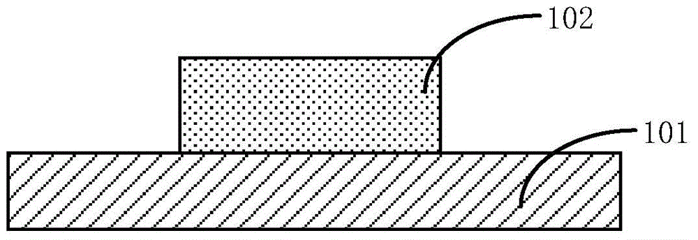
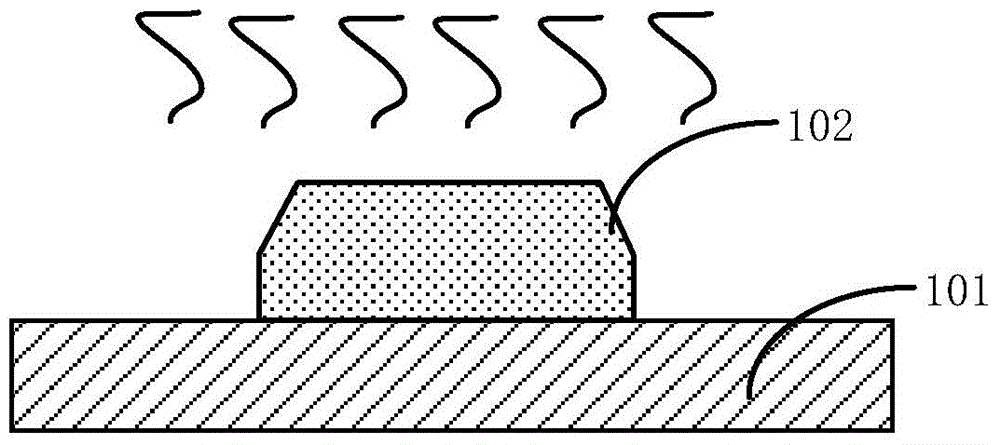
[0040] The first method is photoresist reflow: the commonly used arc-shaped step forming method is to provide a MEMS wafer 101, form a photoresist 102 on the MEMS wafer 101, and form a square or trapezoid on the photoresist graphics, such as Figure 1a As shown, the thermoplastic heating of the photoresist is then used to reflow the photoresist to form a circular arc shape, as shown in Figure 1bshown. Finally, through an etching process, the photoresist pattern is transferred to other materials. This method utilizes the thermoplasticity of the photoresist to heat the photoresist to the melting temperature, so that the photoresist naturally shrinks to form an arc-shaped shape. The disadvantage of this method is that the process of forming an arc-shaped shape is unco...

Embodiment 1

[0044] In order to solve the problems existing in the prior art, the present invention provides a kind of preparation method of MEMS device, below in conjunction with attached Figure 2a-2f The method is described further.

[0045] First, step 201 is performed to provide a MEMS wafer 201 on which a first photoresist layer 202 is formed.

[0046] Specifically, such as Figure 2a As shown, the MEMS wafer 201 can be made of semiconductor materials such as silicon, polysilicon or SiGe, and is not limited to a certain one.

[0047] The MEMS device formed in the present invention may be a sensor, such as a pressure sensor, an acceleration sensor, etc., or a MEMS microphone, or other types of MEMS devices, and is not limited to a certain one.

[0048] Wherein, the first photoresist layer 202 is a photoresist sensitive to a specific wavelength, for example, the first photoresist layer 202 is sensitive to a light source with a first wavelength.

[0049] Further, the wavelength of th...

Embodiment 2

[0086] The present invention also provides a MEMS device, the MEMS device is prepared by the method described in Example 1, the shape of the arc-shaped step in the MEMS device is more controllable, and more in line with the requirements of the design pattern The method solves the problem of uncontrollable arc-shaped steps in the prior art, and further improves the performance and yield of MEMS devices.


PUM


Abstract

The invention relates to a MEMS device, a preparation method and an electronic apparatus. The method comprises the following steps: S1) providing a MEMS wafer, forming a first photoresist layer capable of sensitizing a first wavelength light source on the MEMS wafer; S2) forming a second photoresist layer capable of sensitizing a second wavelength light source on the first photoresist layer for covering the first photoresist layer; S3) selecting the first wavelength light source for exposing the first photoresist layer, selecting the second wavelength light source for exposing the second photoresist layer; and S4) developing the first photoresist layer and the second photoresist layer for forming a first pattern in the first photoresist layer, forming a second pattern in the second photoresist layer, wherein the size of the second pattern is larger than that of the first pattern; and S5) performing heating backflow on the first pattern and the second pattern. The problem of difficult accurate control of photoresist morphology formed by the backflow technology can be solved.

Description

technical field [0001] The invention relates to the field of semiconductors, in particular, the invention relates to a MEMS device, a preparation method thereof, and an electronic device. Background technique [0002] For the increasing demand for high-capacity semiconductor storage devices, the integration density of these semiconductor storage devices has attracted people's attention. In order to increase the integration density of semiconductor storage devices, many different methods have been adopted in the prior art, such as by reducing the wafer size. And / or change the internal structure unit to form multiple memory units on a single wafer. For the method of increasing the integration density by changing the unit structure, attempts have been made to reduce the unit area. [0003] In the field of electronic consumption, multi-function devices are more and more popular among consumers. Compared with devices with simple functions, the production process of multi-functio...

Claims


Application Information

Patent Timeline
IPC IPC(8): B81C1/00B81B1/00G03F7/00G03F7/20
Inventor 刘尧陈福成
Owner SEMICON MFG INT (SHANGHAI) CORP
Learn More