

Organic solar cell comprising nano-bump structure and manufacturing method therefor
An organic photovoltaic cell and nano-concave-convex technology, which is applied in photovoltaic power generation, organic semiconductor devices, circuits, etc., can solve problems such as unsatisfactory organic photovoltaic cells, uncontrollable spacing of nanoparticles, complex nanostructure mask exposure or transmission process, etc. , to achieve the effect of enhanced surface plasmon effect, increased photocurrent, and improved photovoltaic efficiency
- Summary
- Abstract
- Description
- Claims
- Application Information
AI Technical Summary
Problems solved by technology
Method used
Image

Examples
example 1 to example 3
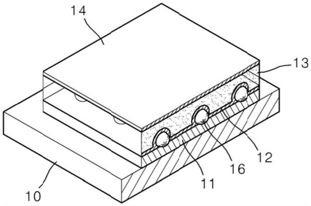
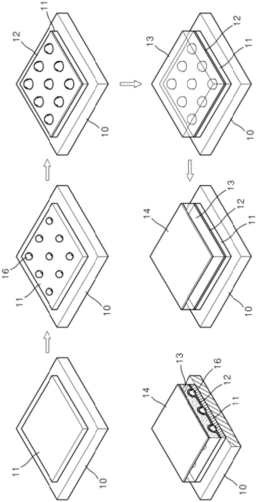
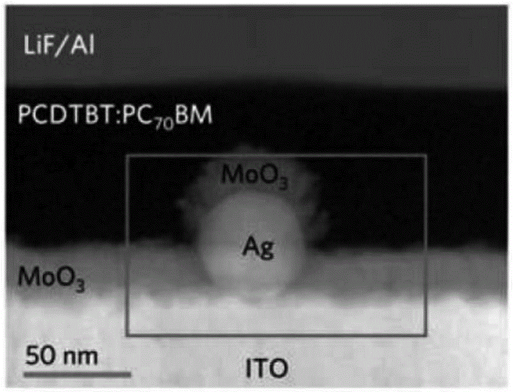
[0070] ITO had a thickness of 150 nm, and was formed by sputtering on a glass substrate having a size of 25 mm x 25 mm and a thickness of 0.7 mm. Silver nanoparticles were bound to the ITO surface as a dry aerosol by an evaporation / condensation process with a size of about 20 nm (Example 1). The molybdenum trioxide is arranged on the exposed part of the silver nanoparticles and the ITO electrode, and the thickness is 20nm, and the molybdenum trioxide and the silver nanoparticles form a nano concave-convex structure. Subsequently, the mixture of PCDTBT and PC70BM (mass ratio 1:4) was spin-coated on the nano-concave-convex structure with a thickness of 90nm, and then lithium fluoride (LIF) and Al To form an electrode, and finally complete the organic photovoltaic cell structure. Organic photovoltaic cell structures were prepared in the same manner as in Example 1, except that the size of the silver nanoparticles was 40 nm (Example 2) and 60 nm (Example 3).
[0071] The evapora...
experiment example 1
[0077] Figure 4a , 4b FE-SEM images (x50,000 magnified image, analysis area 6.0 μm × 4.2 μm) of silver nanoparticles with different sizes (20, 40, and 60 nm) are shown in and 4c, respectively, which show that silver nanoparticles of different sizes The nanoparticles are uniformly and randomly dispersed with a small standard deviation. All analyzes were performed using ImageJ software version 1.46r.
experiment example 2
[0079] J-V characteristics and power conversion efficiencies in the structures prepared in Examples 1, 2 and 3 and Comparative Example 1 were measured under AM1.5G illumination intensity (100 mW / cm2). The result is as Figure 5a with 5b Shown, and the average value is shown in Table 1:
[0080] Table 1:
[0081]
[0082] From Table 1 and Figure 5a with 5b It can be seen that the power conversion efficiency of the structures prepared in Examples 1 to 3 is about 9.5% to 17.6% higher than that of Comparative Example 1. Higher conversion efficiency is used to improve short circuit current (Jsc). The above results indicate that the higher conversion efficiency is due to the enhanced surface plasmon effect induced by the nano-concave-convex structure composed of nanoparticles and covered nanostructures, and the enhanced light absorption due to the uneven structure of the active layer.
PUM
| Property | Measurement | Unit |
|---|---|---|
| height | aaaaa | aaaaa |
| diameter | aaaaa | aaaaa |
| thickness | aaaaa | aaaaa |
Abstract
Description
Claims
Application Information