

Touch display apparatus and fabrication method therefor
A technology of a touch display device and a manufacturing method, which is applied in the directions of instruments, computing, and electrical digital data processing, etc., can solve problems such as defective products, affecting touch sensing functions, and increasing costs, and achieves simplified coating methods and increased coupling area. The effect of large size and simple production process
- Summary
- Abstract
- Description
- Claims
- Application Information
AI Technical Summary
Problems solved by technology
Method used
Image

Examples
no. 1 example
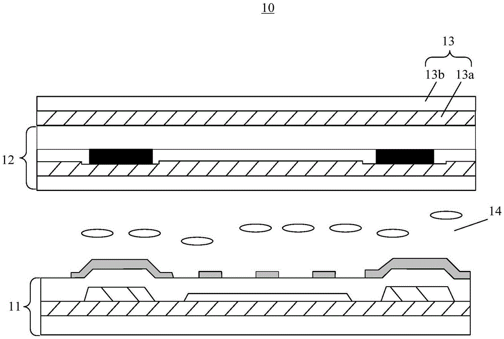
[0034] Figure 2A It is a partial structural schematic diagram of the touch display device provided by the first embodiment of the present invention. Figure 2B yes Figure 2AA schematic diagram of the first electrode of the touch display device. Figure 2C yes Figure 2A A schematic diagram of the second electrode of the touch display device. Figure 2D yes Figure 2A A schematic diagram of the relationship between the first electrode and the second electrode of the touch display device. The touch display device is easy to manufacture, can improve the yield rate of the product, and greatly reduce the cost. Please refer to Figures 2A-2D , the touch display device 100 of this embodiment is an OnCell type touch liquid crystal display device (Liquid Crystal Display, LCD), but it is not limited thereto, for example, it can also be a touch type active matrix organic light emitting diode (ActiveMatrixOrganicLightEmittingDiode, AMOLED ) display device. The touch display devic...
no. 2 example
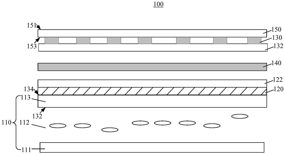
[0044] image 3 It is a schematic structural diagram of the touch display device provided by the second embodiment of the present invention. The difference between this embodiment and FIG. 2 is that the touch display device further includes a flexible circuit board 160 and a touch chip 170 connected to the flexible circuit board 160 .
[0045] Wherein, the flexible circuit board 160 includes two parts, respectively bound on the cover plate 150 and the color filter substrate 113, the first electrode 121 is connected to the binding end of the flexible circuit board 160 on the cover plate 150 through a lead wire, and the cover plate 150 The binding end of the flexible circuit board 160 is also connected to the touch chip 170 . The second electrode 131 is connected to the binding end of the flexible circuit board 160 on the color filter substrate 113 through wires, and the binding end of the flexible circuit board 160 on the color filter substrate 113 is also connected to the tou...
no. 3 example
[0049] Figure 4 is provided by the third embodiment of the present invention such as Figure 2A The flow chart of the manufacturing method of the touch display device. Please refer to Figure 4 , the manufacturing method of the touch display device in this embodiment includes the following steps 401-405.
[0050] Step 401 , fabricating a display substrate 110 . In this embodiment, the display substrate 110 includes an array substrate 111 and a color filter substrate 130 disposed opposite to each other, and a liquid crystal layer 112 sandwiched between the array substrate 111 and the color filter substrate 130 , but not limited thereto. The fabrication steps of the array substrate 111 include fabrication steps of structures such as data lines, scan lines, thin film transistor (ThinFilm Transistor, TFT) arrays, and a transparent protective layer, which will not be repeated here.
[0051] The color filter substrate 113 is disposed above the array substrate 111 , and in this ...
PUM
 Abstract
Description
Claims
Application Information