Solid-state drive control chip integrating MRAM (Magnetic Random Access Memory) and solid-state drive

A solid-state hard disk, control chip technology, applied in the direction of input/output to the record carrier, etc., can solve the problems of data file system damage, system loss, loss, etc., to reduce the number of writes, easy to apply, and prolong life.

Inactive Publication Date: 2016-06-01
SHANGHAI CIYU INFORMATION TECH CO LTD
View PDF6 Cites 12 Cited by
  • Summary
  • Abstract
  • Description
  • Claims
  • Application Information

AI Technical Summary

Problems solved by technology

[0015] However, the introduction of the write cache creates a new problem: Once a power failure occurs, the contents of the DRAM cache that have not been written to the NAND will be lost, causing the system to lose data or even damage the entire file system, so expensive and bulky power failure must be used at the same time Protection system (usually composed of batteries or a large number of capacitors)
[0020] 2 Size: The size of the SSD of the computer is very large, and it is more and more difficult to apply it to the thinner and lighter notebook computer and tablet computer, and it is almost impossible to apply it to the mobile phone;
[0024] However, the control chip does not contain a CPU, and the hard disk uses a physical address. Manufacturers of mobile phones and computers are generally unwilling to directly face the complicated NAND management program and develop drivers for various types of NAND chips, which makes the application of this solution somewhat limited. difficulty

Method used


Image

  • Solid-state drive control chip integrating MRAM (Magnetic Random Access Memory) and solid-state drive
  • Solid-state drive control chip integrating MRAM (Magnetic Random Access Memory) and solid-state drive
  • Solid-state drive control chip integrating MRAM (Magnetic Random Access Memory) and solid-state drive

Examples


Embodiment Construction

[0069] The following are specific embodiments of the present invention and the technical solution of the present invention is further described in conjunction with the accompanying drawings, but the present invention is not limited to the following embodiments.

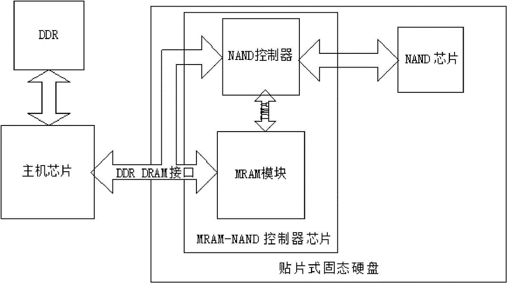
[0070] Such as Figure 4 As shown, the integrated MRAM solid-state hard disk control chip of an embodiment of the present invention includes a CPU, MRAM, a host interface and a NAND controller, the host interface is used to connect the integrated MRAM solid-state hard disk control chip and the host, and the NAND controller is used to control The connection with the NAND chip, the CPU is connected with the MRAM and the NAND controller, and the host interface uses a standard memory read-write interface.

[0071] The solid-state hard disk control chip integrated with MRAM also includes a host interface controller, which is used to control the host interface.

[0072] The solid-state hard disk control chip integrated wit...


PUM


Abstract

The invention provides a solid-state drive control chip integrating an MRAM (Magnetic Random Access Memory). The solid-state drive control chip comprises a CPU, the MRAM, a host interface and an NAND controller, wherein the host interface adopts a standard memory reading and writing interface. The invention furthermore provides a solid-state drive and a corresponding reading and writing method. According to the solid-state drive control chip integrating the MRAM and the solid-state drive, the solid-state drive control chip integrating the MRAM is adopted and the host interface adopts the standard memory interface, so that the reading and writing speed of the solid-state drive is no longer limited by the speed of a serial interface; the reading and writing speed of the solid-state drive is increased; NAND management software is run by the CPU of the solid-state drive control chip integrating the MRAM, so that the technical scheme is easier to apply; due to the adoption of a POP package technology or a 3D SIC technology, the control chip can be used in a mobile phone and a light and thin notebook; and due to the adoption of the MRAM, the writing frequency of an NAND chip is reduced, so that the service life of the NAND chip is prolonged.

Description

technical field [0001] The invention relates to the field of digital storage, in particular to a solid-state hard disk control chip and a solid-state hard disk integrated with MRAM. Background technique [0002] Solid State Drives (SSD), referred to as solid disk, is a device used to store digital information. [0003] The development of NAND flash memory technology has promoted the SSD industry. High-speed serial interfaces such as SATA and PICe are used between SSDs and hosts, such as figure 1 As shown, the interior is composed of a set of NAND chips for storing data, double data rate dynamic random access memory (Double Data Rate Dynamic Random Access Memory, DDRDRAM) for caching data, and a main control chip. [0004] Smartphones also struggle to support SSDs due to their strict size requirements. Generally use a smaller memory card, such as eMMC format or MicroSD format. The structure of the memory card is similar to that of a solid-state drive, except that a large a...

Claims


Application Information

Patent Timeline
Patent Type & Authority Applications(China)
IPC IPC(8): G06F3/06
Inventor 戴瑾
Owner SHANGHAI CIYU INFORMATION TECH CO LTD
Why Eureka
Try Eureka