Central sensor restoration method and central sensor
A repair method and sensor technology, applied in the direction of semiconductor/solid-state device testing/measurement, etc., can solve the problems of performance and function maintenance, debugging, component substitution difficulties, increasing maintenance difficulty, laser diode exit angle, and inability to find laser diodes, etc. The effect of reducing laser power requirements, shortening laser paths, and reducing laser energy consumption
- Summary
- Abstract
- Description
- Claims
- Application Information
AI Technical Summary
Problems solved by technology
Method used
Image

Examples
Embodiment approach
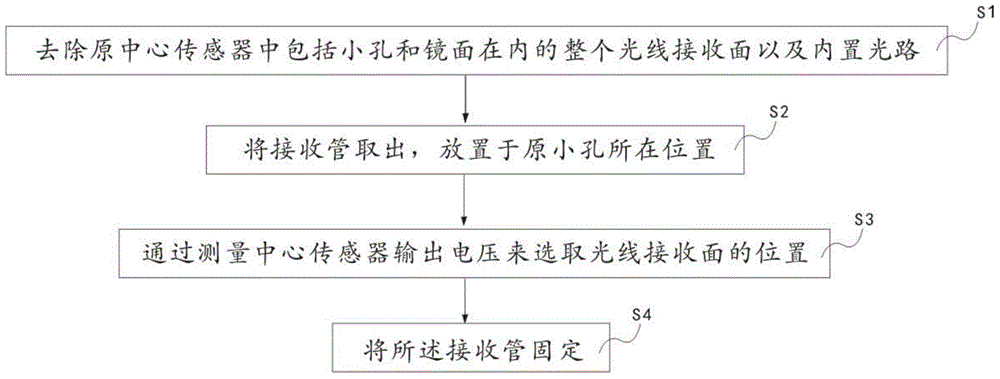
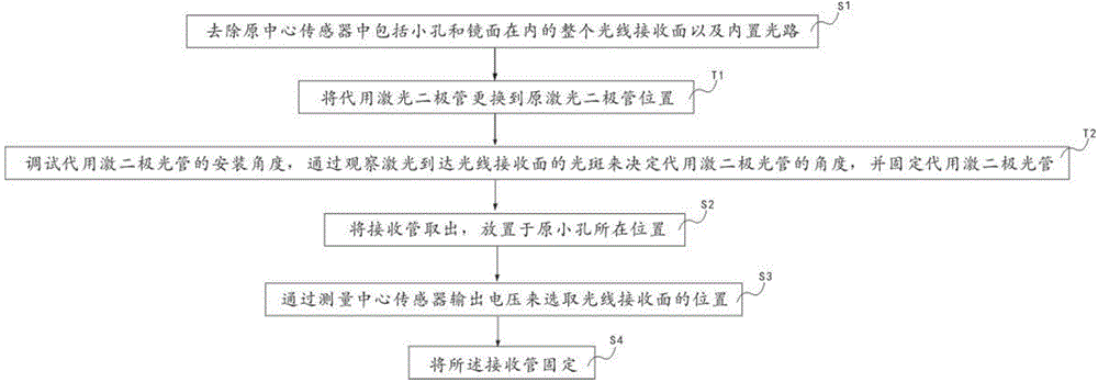
[0032] Such as figure 1 As shown, the first specific embodiment of the present invention firstly provides a repair method for a central sensor, which method includes the following steps:
[0033] Step 1 S1: Remove the entire light-receiving surface including the small hole and the mirror surface and the built-in optical path in the original center sensor.
[0034] In this step, due to the assembly structure of the original central sensor and the firmness of the material, the head must be completely destroyed for the convenience of subsequent steps.
[0035] Step 2 S2: Take out the receiving tube and place it where the original small hole was.
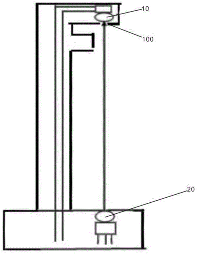
[0036] see figure 2 As shown, the receiving tube 10 (that is, the silicon photocell) is taken out from the original position of the central sensor, and placed in the original position of the small hole 100 . At this time, the direction of the receiving surface of the receiving tube 10 is set downward so as to receive the laser ligh...
PUM
 Abstract
Description
Claims
Application Information
 - Generate Ideas
- Intellectual Property
- Life Sciences
- Materials
- Tech Scout
- Unparalleled Data Quality
- Higher Quality Content
- 60% Fewer Hallucinations
Browse by: Latest US Patents, China's latest patents, Technical Efficacy Thesaurus, Application Domain, Technology Topic, Popular Technical Reports.
© 2025 PatSnap. All rights reserved.Legal|Privacy policy|Modern Slavery Act Transparency Statement|Sitemap|About US| Contact US: help@patsnap.com