Indium bump preparation method and infrared focal plane array detector

An infrared focal plane and indium column technology, which is applied in semiconductor/solid-state device manufacturing, electrical components, circuits, etc., can solve the problems of affecting yield, cracking and falling off of indium film, time-consuming and other problems, so as to improve work efficiency and avoid negative effects. The effect of affecting and shortening the process time

Active Publication Date: 2016-06-01
SUZHOU INST OF NANO TECH & NANO BIONICS CHINESE ACEDEMY OF SCI
View PDF3 Cites 12 Cited by
  • Summary
  • Abstract
  • Description
  • Claims
  • Application Information

AI Technical Summary

Problems solved by technology

At present, the commonly used preparation method of indium column is thermal evaporation indium column combined with wet stripping process, that is, the photoresist mask is dissolved by organic solvent or glue remover, so that the indium film on the mask falls off, but indium is a very " "sticky" metals, the photoresist is easily dissolved, but the indium film sticks back to the chip. Once the metal indium sticks back to the chip, it is difficult to peel it off, which will cause many pixel short circuits and seriously affect device performance; and the wet stripping process generally needs to be soaked in a solvent for a certain period of time, generally more than 1 hour, and then the solvent is heated or ultrasonically vibrated to make the indium film crack and fall off. This method not only takes a long time, but also Moreover, brittle materials such as gallium arsenide in the device are prone to fatal damage such as cracking, which affects the yield

Method used


Image

  • Indium bump preparation method and infrared focal plane array detector
  • Indium bump preparation method and infrared focal plane array detector
  • Indium bump preparation method and infrared focal plane array detector

Examples


Embodiment Construction

[0024] Hereinafter, embodiments of the present invention will be described in detail with reference to the accompanying drawings. This invention may, however, be embodied in many different forms and should not be construed as limited to the specific embodiments set forth herein. Rather, the embodiments are provided to explain the principles of the invention and its practical application, thereby enabling others skilled in the art to understand the invention for various embodiments and with various modifications as are suited to particular intended uses. In the drawings, the shapes and dimensions of elements may be exaggerated for clarity, and the same reference numerals will be used throughout to designate the same or like elements.

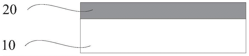
[0025] figure 1 is a flowchart of a method for preparing an indium column according to an embodiment of the present invention.

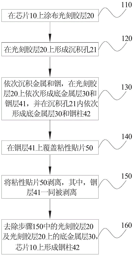
[0026] refer to figure 1 , in step 110 , a photoresist layer 20 is coated on the chip 10 . For the specific metho...


PUM


Abstract

The present invention discloses an indium bump and a preparation method thereof. The preparation method comprises the steps of A, coating a photoresist layer (20) on a chip (10); B, forming a deposition hole (21) on the photoresist layer (20); C, depositing the metal and the indium orderly, forming a bottom metal layer (30) and an indium layer (41) on the photoresist layer (20) orderly, and forming the bottom metal layer (30) and an indium bump (42) in the deposition hole (21) orderly; D, removing the photoresist layer (20) and the bottom metal layer (30) and the indium layer (41) which are located on the photoresist layer (20). The preparation method enables the process time of the indium bump preparation to be shortened and the working efficiency and the indium bump yield to be improved, at the same time, can avoid the fragmentation of the fragile samples, such as the gallium arsenide, etc., in a device. The present invention also discloses the application of the indium bump prepared according to the preparation method in an infrared focal plane array detector, the indium bump can avoid the problems, such as the pixel short circuit caused by a wet stripping technology, etc., and enables the performance of the device to be improved.

Description

technical field [0001] The invention belongs to the technical field of semiconductors, and in particular relates to a preparation method of an indium column, and also relates to an application of the indium column in an infrared focal plane array detector. Background technique [0002] Infrared focal plane array is the core component of modern infrared imaging system, and its manufacturing process includes the preparation of infrared focal plane devices, the preparation of readout circuits, and the flip-chip interconnection of devices and circuits. Flip-chip interconnection generally adopts the flip-chip interconnection of indium pillars. To maximize the success rate of interconnection, it is particularly important to prepare high-quality indium pillars. At present, the commonly used preparation method of indium column is thermal evaporation indium column combined with wet stripping process, that is, the photoresist mask is dissolved by organic solvent or glue remover, so th...

Claims


Application Information

Patent Timeline
Patent Type & Authority Applications(China)
IPC IPC(8): H01L21/768
Inventor 黄宏娟赵德胜张宝顺
Owner SUZHOU INST OF NANO TECH & NANO BIONICS CHINESE ACEDEMY OF SCI
Why Eureka
Try Eureka